Ultra-small LED electrode assembly and method for manufacturing same

a led electrode and ultra-small technology, applied in the direction of sustainable manufacturing/processing, final product manufacturing, programmable/customizable/modifiable circuits, etc., can solve the problems of difficulty in manufacturing, difficulty in manufacturing, difficulty in manufacturing, etc., to improve light extraction efficiency

Active Publication Date: 2016-05-26
SAMSUNG DISPLAY CO LTD
View PDF6 Cites 57 Cited by
  • Summary
  • Abstract
  • Description
  • Claims
  • Application Information

AI Technical Summary

Benefits of technology

[0015]The present invention provides a method for manufacturing a nano-scale LED electrode assembly, in which an independently manufactured nano-scale ELD device having a nano unit, is connected to two electrodes different from each other without causing defects such as an electrical short-circuit to improve light extraction efficiency.

Problems solved by technology

However, it is difficult to manufacture the blue LED device having high efficiency.
Drawbacks in improvement of efficiency of the blue LED device may cause the difficulty in manufacturing and a high refractive index between the manufactured LED and the GaN-based semiconductor.
First, the difficulty in the manufacturing may be caused due to the difficulty in manufacturing of a substrate having the same lattice constant as the GaN-based semiconductor.
A GaN epitaxial layer formed on the substrate may have many defects when the lattice constant with the substrate is significantly mismatched to deteriorate efficiency and reduce performance.
The former method may have a limitation in that it is very difficult to crystallographically grow of high crystalline / high efficiency thin film and LED device, and the latter method may have a limitation in that light extraction efficiency is reduced to deteriorate light emitting efficiency.
Also, according to the latter method, although a three-dimensional LED device is connected to the electrode in a stand-up state in case of the general LED device, it is very difficult to stand up on the electrode in case of a nano-scale LED device having a nano unit.
However, it is very difficult to couple the nano-scale LED device to the electrode in the three-dimensionally stand-up state.
However, in case of the nano-scale LED device, it is very difficult to respectively locate the LED devices on two nano-scale electrodes different from each other within a desired range.
Also, even though the LED devices are disposed on the two nano-scale electrodes, defects such as electrical short-circuit between the electrode and the nano-scale LED may frequently occur, and it may be difficult to realize the desired electrode assembly.
However, if the mounted LED chip has a nano size, it may be very difficult to accurately mount the three-dimensional LED chip on the upper electrode.
Also, even though the LED chip is mounted on the upper electrode, it may be very difficult to connect the mounted LED chip having the nano size to the lower electrode.
In addition, since n-type and p-type semiconductor layers of the mounted LED chip form upper and lower layers with respect to a substrate, light emitted from the active layer may be blocked by the LED chip and thus may not be escaped, but be absorbed to the inside, thereby deteriorating light extraction efficiency.

Method used


Image

  • Ultra-small LED electrode assembly and method for manufacturing same
  • Ultra-small LED electrode assembly and method for manufacturing same
  • Ultra-small LED electrode assembly and method for manufacturing same

Examples


example 1

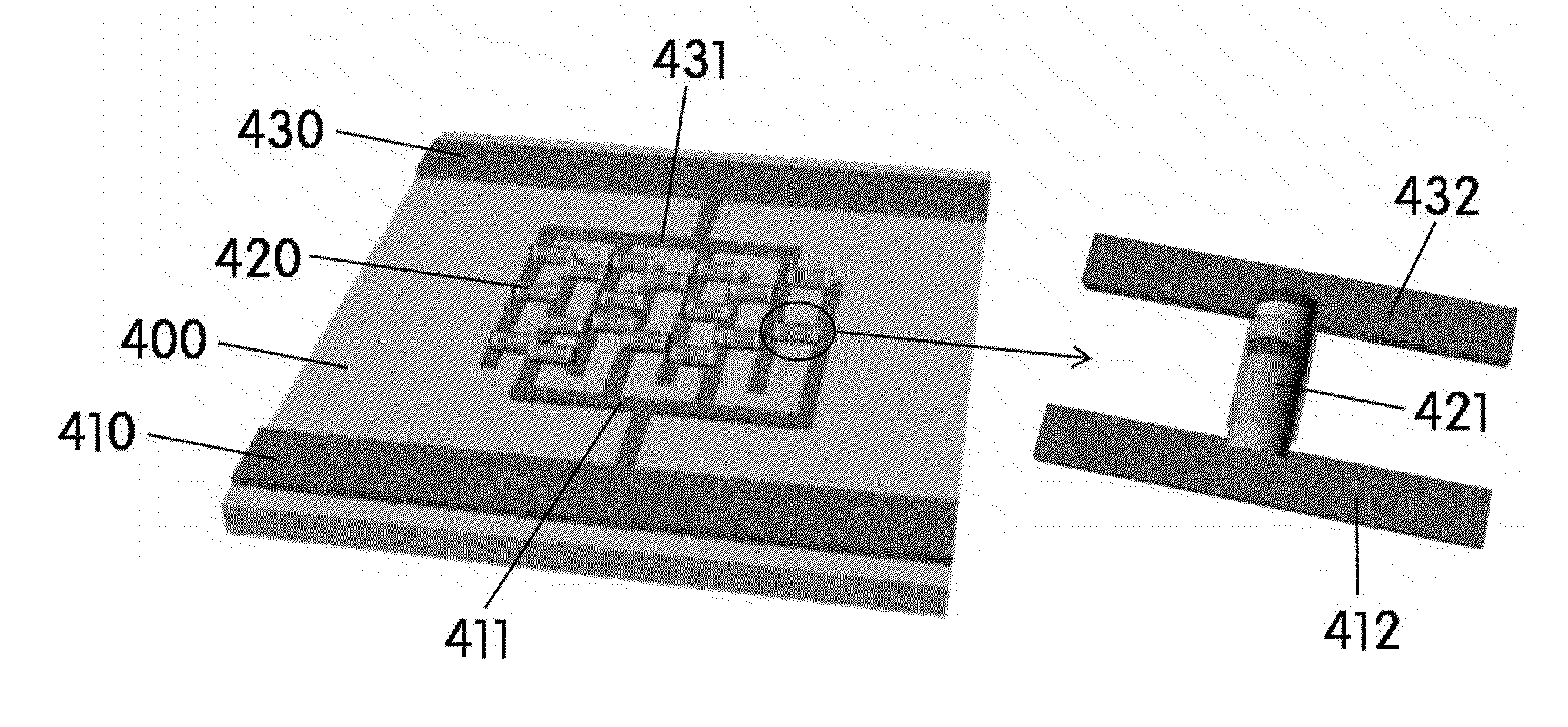
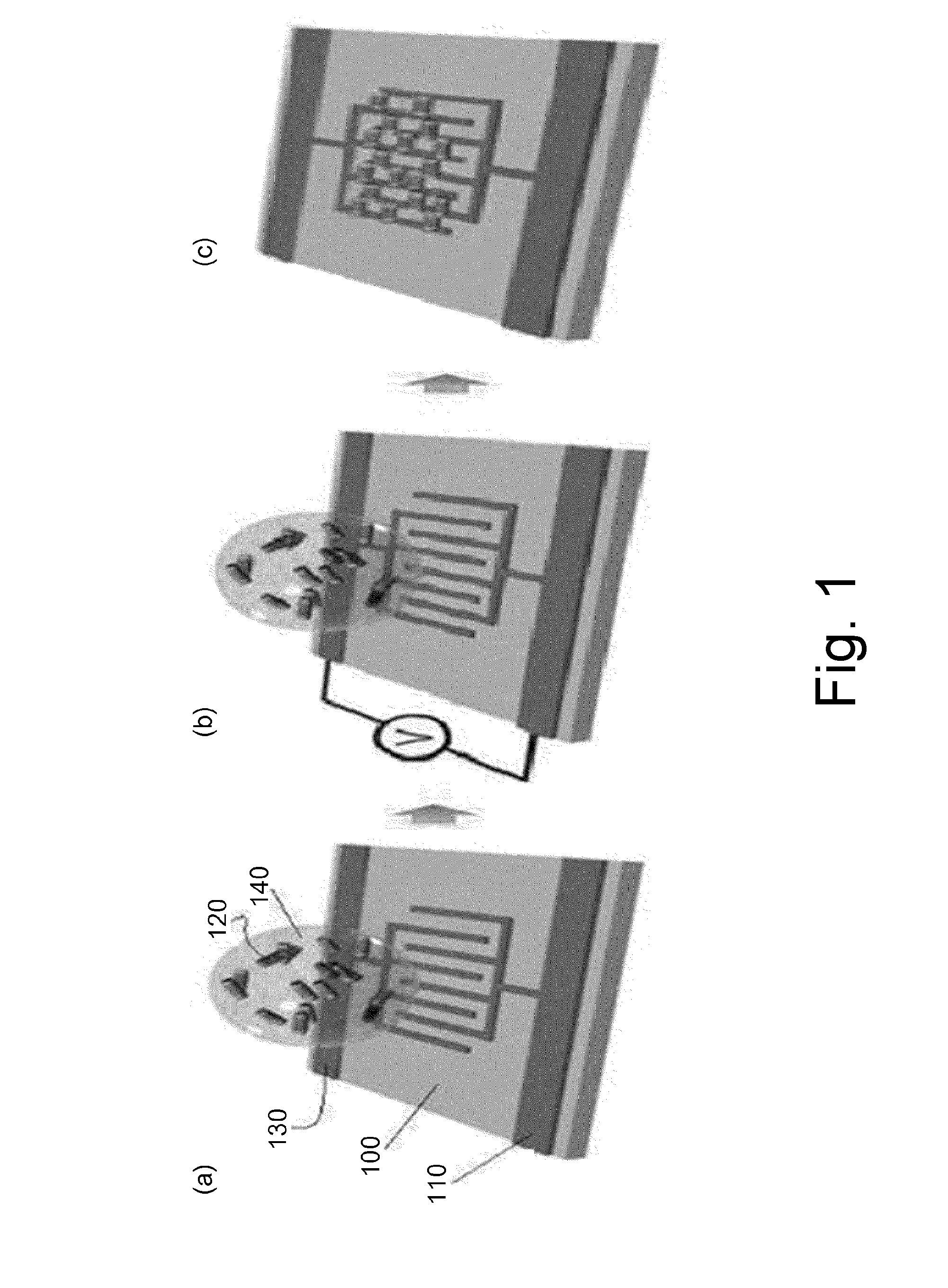
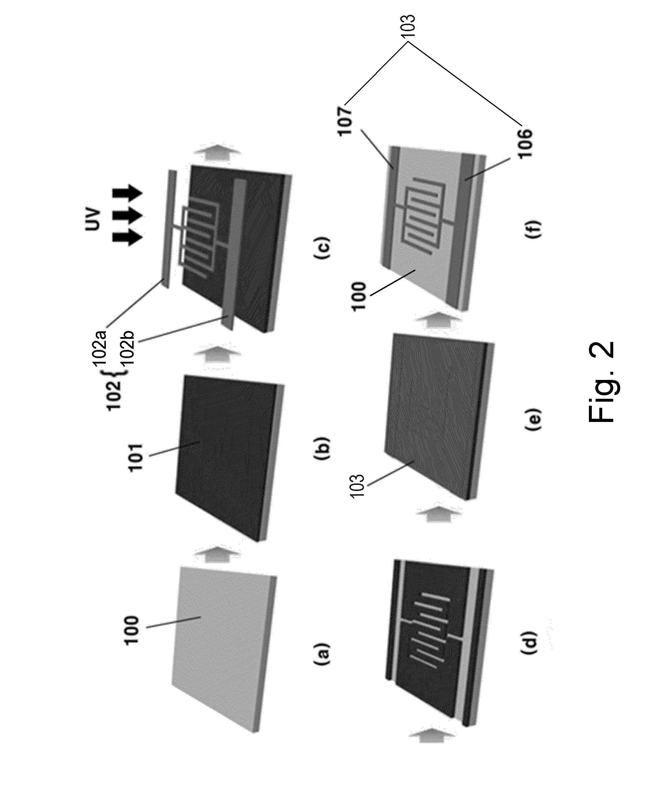
[0204]An electrode line as illustrated in FIG. 3 was manufactured on a base substrate formed of quartz and having a thickness of about 800 μm. Here, in the electrode line, a first electrode has a width of about 3 μm, a second electrode has a width of about 3 μm, a distance between the first electrode and the second electrode is about 2 μm, and each of the electrodes has a thickness of about 0.2 μm. Also, each of the first and second electrodes is formed of a titanium / gold material, and an electrode line region on which the nano-scale LED device has an area of about 4.2×107 μm 2. Thereafter, an insulation barrier as illustrated in FIG. 9 was formed on the base substrate. The insulation barrier was formed of silicon dioxide, and a height from the base substrate to an end of the insulation barrier is about 0.1 μm. Here, the insulation barrier was formed on the base substrate except for the region (area of 4.2×107 μm 2) in which the nano-scale LED device is mounted on the electrode line...

example 2

[0207]Although the same process as Example 1 is performed, the insulation barrier was not formed, and nano-scale LED devices dropped onto an electrode line formed on a base substrate which does not include the insulation barrier to manufacture a nano-scale LED electrode assembly.

example 3

[0208]Although the same process as Example 1 is performed, nano-scale LED devices were injected to an electrode line region, instead that the solution containing the nano-scale LED devices drops to the electrode line region surrounded by the insulation barrier on the base substrate. Then, acetone was injected to the region on which the nano-scale LED devices are injected. Here, the injected acetone has about 10,000 weight parts with respect to 100 weight parts of the nano-scale LED devices. While the solvent is injected, AC power having a voltage of VAC=30 V and a frequency of about 950 kHz was applied to the electrode line for one minute to manufacture the nano-scale LED electrode assembly.


PUM


Abstract

Provided are a nano-scale LED assembly and a method for manufacturing the same. First, a nano-scale LED device that is independently manufactured may be aligned and connected to two electrodes different from each other to solve a limitation in which a nano-scale LED device having a nano unit is coupled to two electrodes different from each other in a stand-up state. Also, since the LED device and the electrodes are disposed on the same plane, light extraction efficiency of the LED device may be improved. Furthermore, the number of nano-scale LED devices may be adjusted. Second, since the nano-scale LED device does not stand up to be three-dimensionally coupled to upper and lower electrodes, but lies to be coupled to two electrodes different from each other on the same plane, the light extraction efficiency may be very improved. Also, since a separate layer is formed on a surface of the LED device to prevent the LED device and the electrode from being electrically short-circuited, defects of the LED electrode assembly may be minimized. Also, in preparation for the occurrence of the very rare defects of the LED device, the plurality of LED devices may be connected to the electrode to maintain the original function of the nano-scale LED electrode assembly.

Description

CROSS-REFERENCE TO RELATED APPLICATIONS[0001]This U.S. non-provisional patent application claims priority under 35 U.S.C. §119 of Korean Patent Application No. 10-2013-0080417, filed on Jul. 9, 2013, the entire contents of which are hereby incorporated by reference.BACKGROUND OF THE INVENTION[0002]The present invention disclosed herein relates to a nano-scale LED electrode assembly and a method for manufacturing the same, and more particularly, to a nano-scale LED electrode assembly in which a nano-scale LED device having a nano unit is connected to a nano-scale electrode without causing defects such as an electrical short-circuit while maximizing light extraction efficiency and a method for manufacturing the same.[0003]The development of light emitting diodes (LEDs) has been actively promoted by succeeding in combination of a high-quality single-crystal gallium nitride (GaN) semiconductor by applying a low-temperature GaN compound buffer layer, by Nakamura et al., at Nichia Chemica...

Claims


Application Information

Patent Timeline
Patent Type & Authority Applications(United States)
IPC IPC(8): H01L25/075H01L33/38H01L33/62
CPCH01L25/0753H01L2933/0066H01L33/38H01L33/62H01L2924/0002H05K1/0295H05K1/0296H05K1/111H05K3/3442H05K2201/09236H05K2201/09254H05K2201/09381H05K2201/0939H05K2201/09427H05K2201/09954H05K2201/10106H05K2201/10583H05K2201/10636H05K2201/10651H05K2203/048Y02P70/50H01L2924/00
Inventor DO, YOUNG RAG
Owner SAMSUNG DISPLAY CO LTD
Why Eureka
Try Eureka