Three dimensional sub-mm wavelength sub-thz frequency antennas on flexible and uv-curable dielectric using printed electronic metal traces

Active Publication Date: 2016-06-16
WASHINGTON STATE UNIVERSITY
View PDF3 Cites 32 Cited by
  • Summary
  • Abstract
  • Description
  • Claims
  • Application Information

AI Technical Summary

Benefits of technology

[0011]Accordingly, the embodiments herein provide for three-dimensional passives and antenna structures on soft substrates that are beneficial to a host of internet-ready devices including wearable sensing, biometric and communication devices, implants, and chip-to-chip communication, etc. Flexible electronics with wireless sensing are at the hear

Problems solved by technology

In addition, the number of 3D shapes are rather limited.
Finally, the degree of folding of Origami is difficult to control due to the inherent structural instabilities and the nonlinear stress/strain response of these structures, leading to an unpredictable response over the operating frequencies in the case of its use in antennas.
The approach in (b) suffers from the fact that the met

Method used


Image

  • Three dimensional sub-mm wavelength sub-thz frequency antennas on flexible and uv-curable dielectric using printed electronic metal traces
  • Three dimensional sub-mm wavelength sub-thz frequency antennas on flexible and uv-curable dielectric using printed electronic metal traces
  • Three dimensional sub-mm wavelength sub-thz frequency antennas on flexible and uv-curable dielectric using printed electronic metal traces

Examples


examples

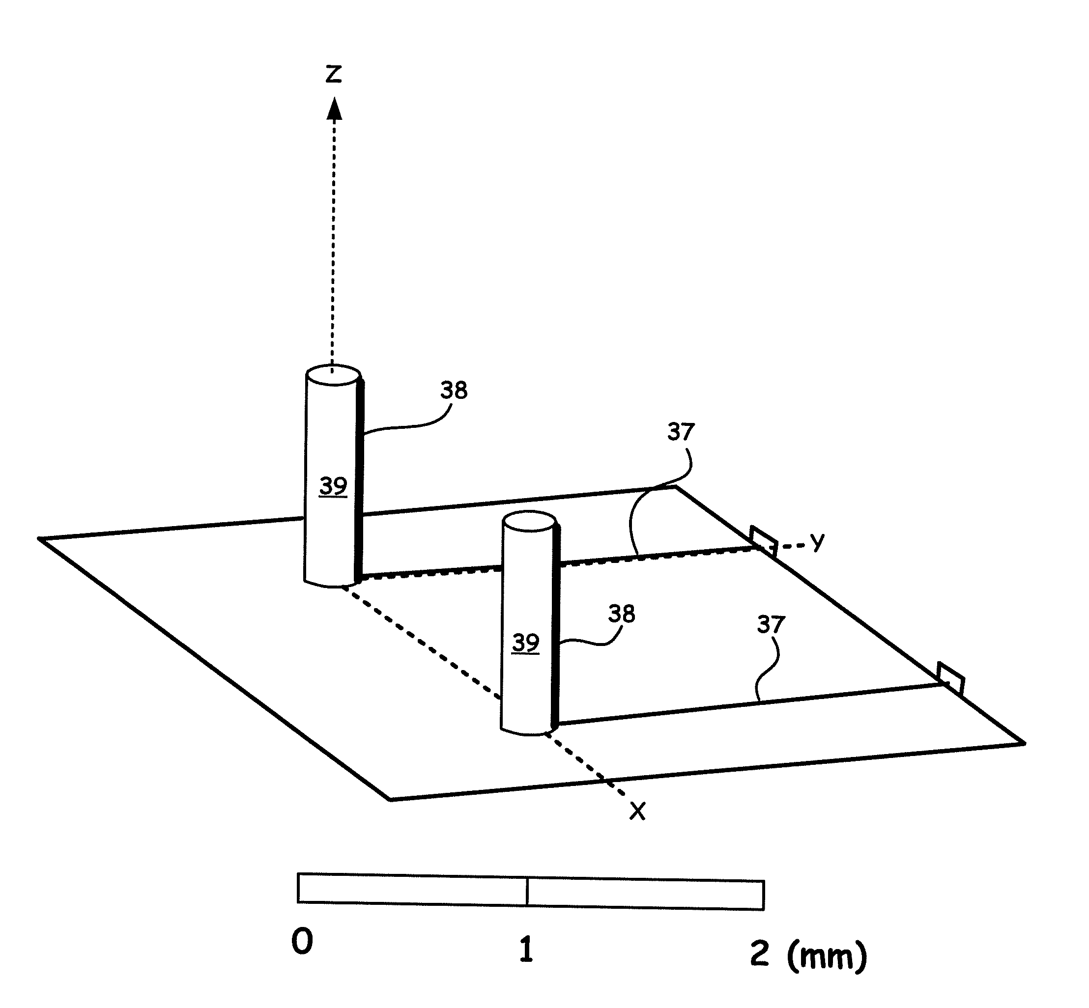
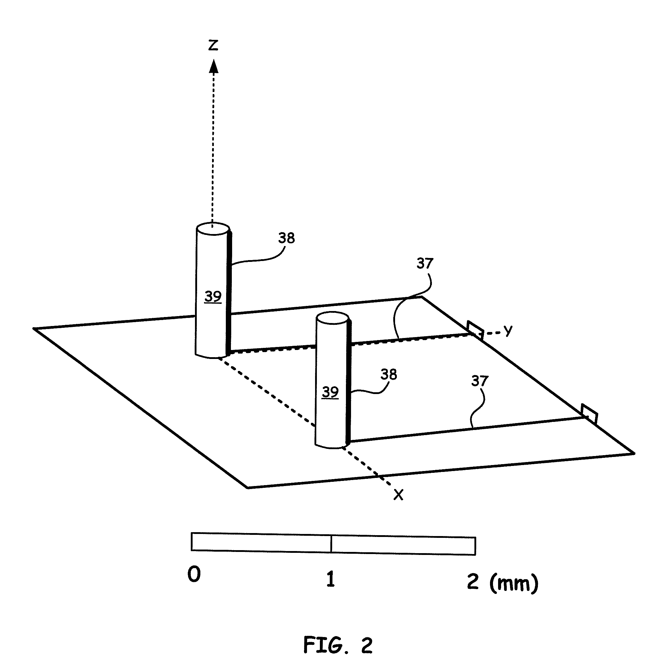
[0069]Beneficial Example Materials

[0070]The primary material sets used to create 3D antenna-like structures exemplified in FIGS. 5A-5E and FIGS. 6A-6D include a metallic nanoparticle ink and a UV curable dielectric. Silver nanoparticle ink is desirably used (Advanced Nano Particle Inc., Fremont, Calif., AS1:2), while the dielectric material used is a UV curable Acrylic Urethane (Loctite 3105, Henkel Inc.). The size of the metal nanoparticles had about 50 wt %±5% particle loading with particle size of 50-100 nm with a viscosity of about 160 cP at 0.4 rpm. The dielectric material has a viscosity of 300 cP. A minimum nanoparticle curing regimen was applied at 130° C. / 2 h. The resistivity measured in these conditions is about 9×10⁻⁸ Ωm or about 20% of the bulk silver (Optomec data sheet). Glass and a functional Si chip were used as the substrate. The substrates were cleaned with DI water followed by isopropyl alcohol. An atmospheric plasma at 100 W for 1 min was then applied to the subs...


PUM

PropertyMeasurementUnit
Lengthaaaaaaaaaa
Angleaaaaaaaaaa
Lengthaaaaaaaaaa

Abstract

Novel methods for micro-additive manufacturing three dimensional sub-millimeter components are disclosed herein. The methods can include dispensing a dielectric at positions on a substrate so as to provide dielectric structures having an aspect ratio of up to 1:20. The methods can also include in-situ curing of the dielectric structure upon dispensing of the dielectric wherein the dispensing and curing steps provide for three dimensional configurations. Direct printing a metal nanoparticle solution on the dielectric to create conductive traces and thereafter sintering the printed nanoparticle solution so as to cure the conductive traces enables three dimensional conductive (antenna) elements having a length and width scale of down to 1 μm.

Description

CROSS-REFERENCE TO RELATED APPLICATION(S)[0001]The present application claims under 35 U.S.C. §119, the priority benefit of U.S. Provisional Application No. 62 / 090,319, filed Dec. 10, 2014. The disclosure of the foregoing application is incorporated herein by reference in its entirety.BACKGROUND OF THE INVENTION[0002]1. Field of the Invention[0003]The present disclosure relates to the fabrication of electrical components and circuits, and more particularly to a system and method for forming three dimensional sub-mm frequency antennas on flexible and in-situ cured dielectric material along with directly printed metallic antenna elements over the dielectric.[0004]2. Discussion of the Related Art[0005]The continual drive for smaller, more powerful, and more economical electronic systems led to the development of new manufacturing technologies. In particular, the fabrication of three-dimensional (3D) metal-dielectric structures at sub-mm length scale is highly important in order to real...

Claims


Application Information

Patent Timeline
IPC IPC(8): H01P11/00
CPCH01P11/001B22F7/08B22F2999/00H05K1/0284H05K3/1241H05K2201/10098H05K2203/0126B29C70/882B33Y80/00Y10T29/49155Y10T29/49016Y10T29/49124B33Y10/00B33Y50/02H01G4/1218Y02P10/25B22F10/10B22F12/10B22F10/322B22F12/33B22F1/054H05K1/097B22F1/07G06F1/163H01F27/24H01F27/2804H01F41/0206H01F41/046H05K1/028H05K1/0283H05K1/0296H05K1/0313H05K1/0393H05K1/09H05K3/14H05K3/22H05K3/4644H05K2201/0162
Inventor PANAT, RAHULHEO, DEUK HYOUN
Owner WASHINGTON STATE UNIVERSITY
Why Eureka
Try Eureka