Conductive film and production method thereof

a technology of conductive film and production method, which is applied in the direction of conductive layer on insulating support, packaging, synthetic resin layered products, etc., can solve the problems of degrading the optical property of the conductive film and the difficulty of removing the bubbles generated therein, and achieve excellent peeling strength

Active Publication Date: 2016-06-30
LG CHEM LTD
View PDF8 Cites 1 Cited by
  • Summary
  • Abstract
  • Description
  • Claims
  • Application Information

AI Technical Summary

Benefits of technology

[0010]According to the present application, a conductive film, which does not have bubbles generated by thermal treatment in a manufacturing process, and thus an optical property is degraded, can be provided. Particularly, a conductive film that does not have bubbles even with conductive layers formed on both sides thereof, a use thereof, and a method of manufacturing the same can be provided.
[0011]Also, in the present application, a conductive film including a conductive base layer having an excellent peel strength with respect to an intermediate base layer, a use of the conductive film, and a method of manufacturing the same can be provided.
[0012]FIGS. 1 and 2 are schematic diagrams illustrating a process of manufacturing a transparent conductive film by attaching a conductive base layer before a layer of a pressure-sensitive adhesive composition of the present application is crosslinked.
[0013]FIG. 3 is a schematic diagram illustrating a process of manufacturing a transparent conductive film by attaching a conductive base layer after a pressure-sensitive adhesive layer is formed by crosslinking a layer of a pressure-sensitive adhesive composition of the present application.
[0014]FIG. 4 is a schematic diagram illustrating a process of manufacturing a transparent conductive film, which is manufactured by attaching a conductive base layer before a layer of a pressure-sensitive adhesive composition of the present application is crosslinked and performing crosslinking.
[0015]FIGS. 5 and 6 are schematic diagrams illustrating a thermal treatment for crosslinking a layer of a pressure-sensitive adhesive composition.

Problems solved by technology

Particularly, when the conductive layer is formed on a plastic film, and the thermal treatment is performed at a high temperature, due to the influence of a low molecular weight component such as an oligomer existing in the plastic film, bubbles may be generated in the conductive film, and such bubbles become a cause of degrading an optical property of the conductive film such as transparency.
Particularly, when the conductive layers are formed on both sides of the film, they serve as a barrier to the bubbles, and therefore it is more difficult to remove the bubbles generated therein.

Method used


Image

  • Conductive film and production method thereof
  • Conductive film and production method thereof
  • Conductive film and production method thereof

Examples


example 1

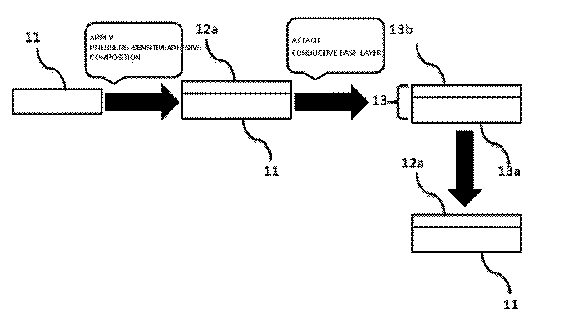
[0110]A pressure-sensitive adhesive composition was prepared by mixing a mixture solution including 94 parts by weight of butyl acrylate (BA) and 6 parts by weight of acrylic acid (AA) with 1 part by weight of a toluene diisocyanate crosslinking agent with respect to 100 parts by weight of the mixture solution. A pressure-sensitive adhesive layer was formed by directly applying the pressure-sensitive adhesive composition to both sides of a polyethyleneterephthalate base layer, and dividing the polyethyleneterephthalate to which the pressure-sensitive adhesive composition was applied into four sections and then drying the polyethyleneterephthalate at 80 to 140° C. in an oven. A double-side conductive film was manufactured by attaching a conductive base layer by means of the pressure-sensitive adhesive layer formed on both sides of the polyethyleneterephthalate. A peel strength of the double-side conductive film is as shown in Table 1 below. Also, the double-side conductive film was a...

example 2

[0111]A pressure-sensitive adhesive composition was prepared by mixing a mixture solution including 94 parts by weight of butyl acrylate (BA) and 6 parts by weight of acrylic acid (AA) with 1 part by weight of a toluene diisocyanate crosslinking agent with respect to 100 parts by weight of the mixture solution, and the double-side conductive film was manufactured by the same method as described in Example 1. Peel strengths of the double-side conductive film and detection results for bubbling are shown in Tables 1 and 2 below.

example 3

[0112]A pressure-sensitive adhesive composition prepared by mixing a mixture solution including 50 parts by weight of 2-ethylhexyl acrylate, 40 parts by weight of methyl acrylate and 10 parts by weight of 2-hydroxyethyl acrylate with 0.25 parts by weight of an isocyanate crosslinking agent with respect to 100 parts by weight of the mixture solution was directly applied to both sides of a polyethyleneterephthalate base layer, and then a conductive film was manufactured by the same method as described in Example 1. Peel strengths of the double-side conductive film and detection results for bubbling are shown in Tables 1 and 2 below.


PUM

PropertyMeasurementUnit
temperature peel strengthaaaaaaaaaa
temperatureaaaaaaaaaa

Abstract

The present application relates to a conductive film, a production method for the same, and a use of the same. The present application is capable of providing, for example, a conductive film without air bubbles, etc. which are generated by heat treatment, etc. during a production process, and inhibit optical physical properties. In particular, the present application can provide a conductive film without generation of air bubbles even in a structure in which the conductive layers exist on both sides of the conductive film.

Description

CROSS-REFERENCE TO RELATED APPLICATION[0001]This application claims priority to and the benefit of Korean Patent Application No. 2013-0097222, No. 2013-0097223 and No. 2013-0097224, filed on Aug. 16, 2013, the disclosure of which is incorporated herein by reference in its entirety.TECHNICAL FIELD[0002]The present application relates to a conductive film, a use thereof, and a method of manufacturing the same.BACKGROUND ART[0003]A conductive film represented by an indium tin oxide (ITO) film is being used in various applications, for example, an electrode for a display device such as a plasma display panel (PDP) or a liquid crystal display (LCD), or an organic light emitting diode (OLED), and an electrode for a touch panel.[0004]The conductive film may be manufactured by forming a conductive layer like ITO on one or both sides of a glass substrate or plastic film by a method such as deposition and the like.[0005]In order to crystallize the conductive layer such as ITO in the manufactu...

Claims


Application Information

Patent Timeline
Patent Type & Authority Applications(United States)
IPC IPC(8): H01B5/14H01B13/00B32B7/12
CPCH01B5/14B32B2307/202H01B13/0026B32B7/12G06F2203/04103C09J133/08C08F220/1808C08F220/14C08F220/20C08F220/1804C08F220/06
Inventor WOO, DONG HYUNYANG, SE WOOPARK, MIN SOOHWANG, JI YOUNG
Owner LG CHEM LTD
Why Eureka
Try Eureka