An electrode for an organic electronic device
an electronic device and electrode technology, applied in the field of electrodes for organic electronic devices, can solve the problems of large light intensity drop, high resistivity, and unsuitable uniformity, and achieve the effects of improving adhesion, and reducing the number of electrodes
- Summary
- Abstract
- Description
- Claims
- Application Information
AI Technical Summary
Benefits of technology
Problems solved by technology
Method used
Image
Examples
example 1
Comparison of Cu Only and Au Only Devices
[0287]Comparable devices were prepared according to the above methods, wherein the light emitting layer was LEP1. The electrical performance of each of the devices is summarised in the table below and shown in FIGS. 4(a)-(d) (LEP2) and FIGS. 5(a)-(c) (LEP1).
MedianMedian efficiencyMedianefficiency(Cd / A) @EQE @(Lm / W) @Median100010001000lifetimeDeviceCd / m2Cd / m2Cd / m2(hrs)Au only57.116.032.7LEP2Cu only53.815.128.3LEP2Au only27.919.6590LEP1Cu only18.48.8140LEP2
[0288]The results show that unprotected copper leads to a significant drop in device performance. Current density, EQE and Lm / W all drop significantly when Cu is used as an anode compared to the unreactive, but expensive, Au anode metal. In all cases the Cu devices short on lifetest very rapidly, and the Au devices live on to T70 in most cases.
example 2
Impact of Acetic Acid Rinse Step
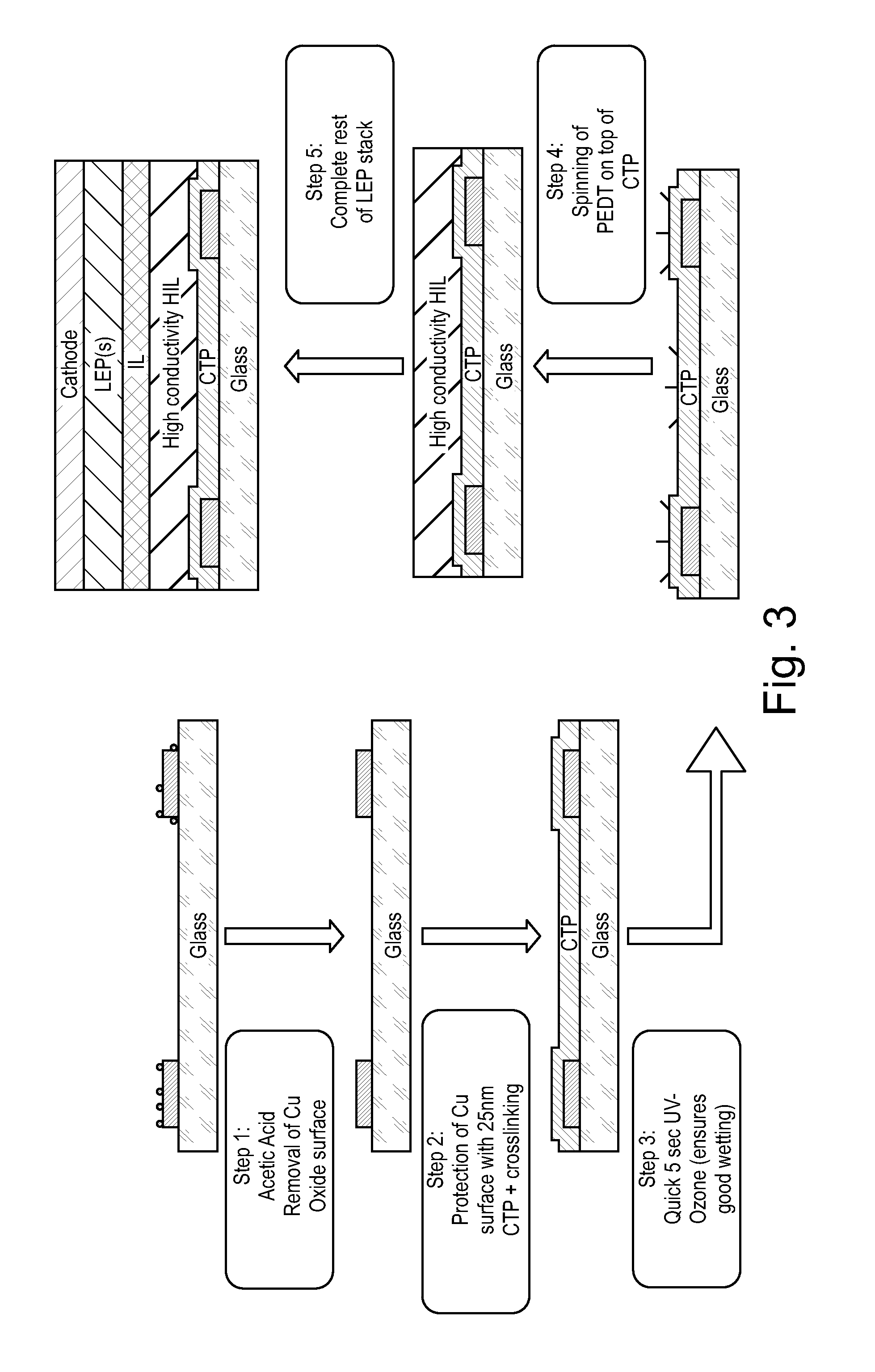
[0289]Comparable devices were prepared according to the above methods, wherein the light emitting layer was LEP1. An acetic acid rinse step was employed prior to deposition of the HIL. Thus the copper grid was treated with 2M acetic acid and heated to 60° C. for 1 minute to remove any CuO from the surface. The substrates were then dried under N2 air and transferred into a glove box (N2 environment) and baked at 70° C. for 15 minutes. The electrical performance of each of the devices is summarised in the table below and shown in FIGS. 6(a)-(c). The table additionally includes comparable data for the Cu only devices, i.e. devices wherein the acetic acid rinse step was not carried out as in example 1 above.
MedianMedianMedianMedianvoltagecurrentefficiencyefficiency(V) @(mA / cm2) @(Cd / A) @(Lm / W) @1000100010001000DeviceCd / m2Cd / m2Cd / m2Cd / m2Au only4.53.627.919.6Cu with acetic6.64.820.910.1acid rinseCu only6.75.418.48.8
[0290]The results show that the use of an ...
example 3
Impact of Protective Charge Transporting Polymer Layer on the Cu Anode
[0291]A series of three experiments were carried wherein comparable devices were prepared according to the above methods and as summarised in the table below. All protective charge transporting polymer layers had a thickness of 25 nm. An UV / ozone treatment and acetic acid rinse step were employed as described above prior to deposition of the HIL. The electrical performance of each group of devices is summarised in the table below and shown in FIGS. 7(a)-(d).
ProtectiveMedianMedianMedianMedianchargevoltage currentefficiency efficiencyMediantransporting(V) (mA / cm2)(Cd / A) (Lm / W)EQE Medianpolymer@ 1000@ 1000@ 1000@ 1000@ 1000lifetimeAnodelayerCd / m2Cd / m2Cd / m2Cd / m2Cd / m2(hrs)Au—5.23.429.317.711.9475CuCTP15.03.429.718.612.290Cu—6.03.627.714.311.1Au—4.93.330.319.512.5CuCTP55.23.627.916.711.6CuCTP65.33.826.715.811.1Au—4.73.826.517.810.1CuCTP35.14.025.215.89.4CuCTP44.83.727.117.310.6
[0292]The results show a significant improv...
PUM
| Property | Measurement | Unit |
|---|---|---|
| width | aaaaa | aaaaa |
| thickness | aaaaa | aaaaa |
| wavelength | aaaaa | aaaaa |
Abstract
Description
Claims
Application Information


