


Quick Research
Generate reliable direction feasibility study reports for your R&D in just a few steps.

Technical Q&A
Discover and master advanced knowledge NOW. Basics, ideas, possibilities, all at once.

Find Solutions
As an expert in R&D theories, this can generate solutions to your technical problems instantly.

Evaluate Feasibility
Analyze your overall solution with one click, know your potential R&D risks in advance.

Monitor Landscape
Get weekly tech updates, stay abreast of the latest tech innovations and key insights.
Composition for forming conductive pattern and resin structure having conductive pattern thereon
- Summary
- Abstract
- Description
- Claims
- Application Information
AI Technical Summary
Benefits of technology
Problems solved by technology
Method used
Image

Examples
preparation example 1
Synthesis of Non-Conductive Metal Compound CuSn2(PO4)3
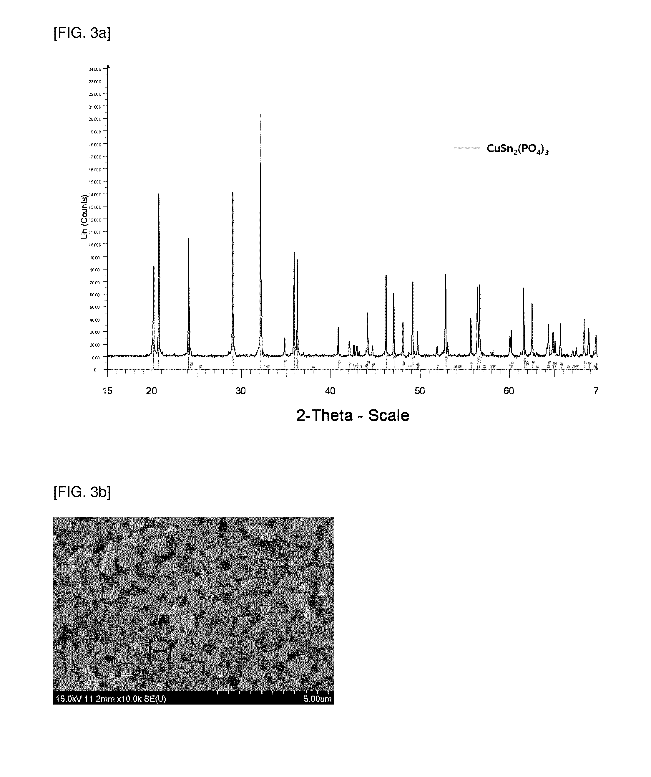
[0075]Copper pyrophosphate and tin pyrophosphate were mixed in a stoichiometric ratio, and fired at about 1100° C. for 3 hours, to synthesize a non-conductive metal compound CuSn2(PO4)3 by a solid state reaction.
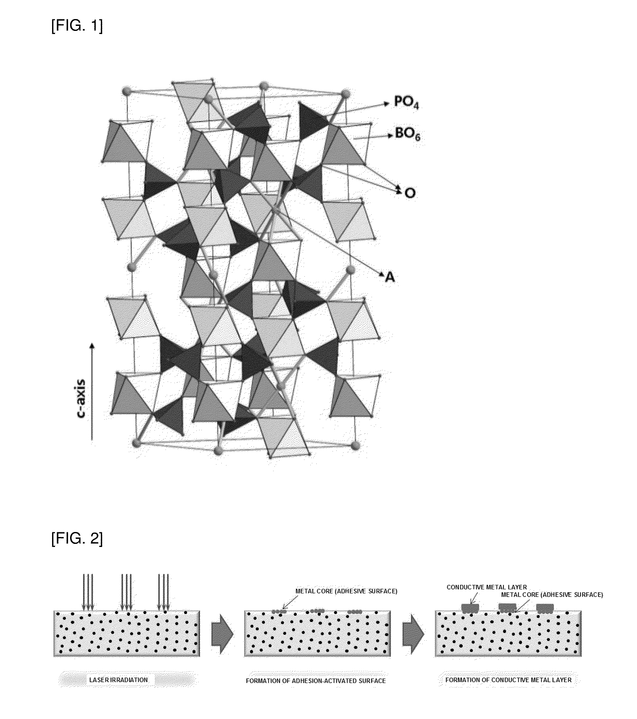
[0076]The XRD pattern and the electron microscope image of the synthesized compound are shown in FIG. 3a and FIG. 3b. As a result of analysis of XRD structure, it was confirmed that the CuSn2(PO4)3 synthesized in Preparation Example 1 has a NASICON crystal structure.
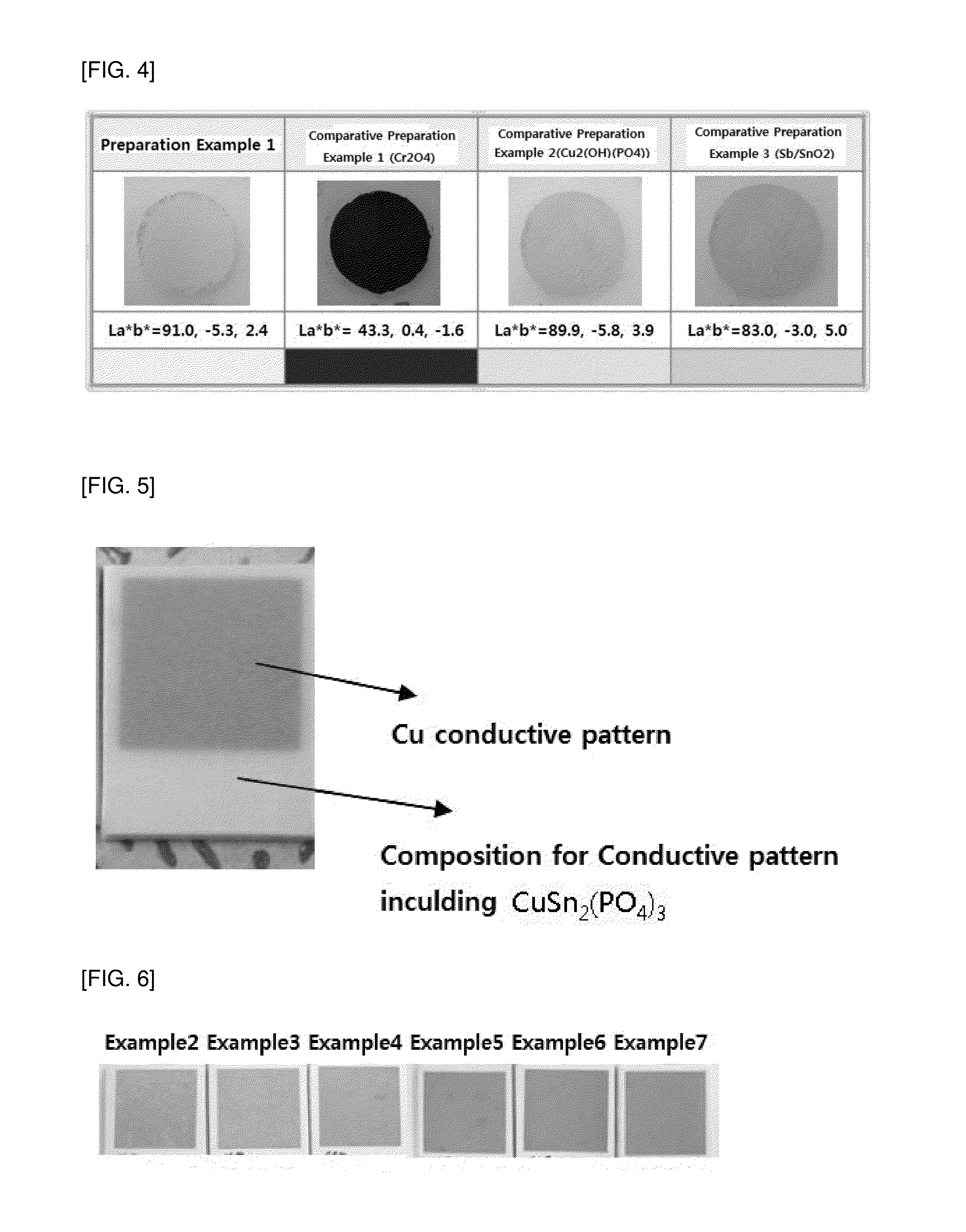
[0077]According to the standard method of ASTM 2244, using a color coordinate measuring device of X-rite color eye 7000A, CIE Lab color coordinate of Preparation Example 1 was measured, and the measurement result is shown together with the photograph of the non-conductive metal compound of Preparation Example 1 in FIG. 4. As a result of the measurement, it was confirmed that the non-conductive metal compound of Preparation Example 1 has a color coordinate of ...
preparation example 2
Synthesis of Non-Conductive Metal Compound AgSn2(PO4)3
[0078]Silver nitrate, tin chloride and phosphoric acid were mixed in a stoichiometric ratio, and fired at about 900° C. for 2 hours, to synthesize a non-conductive metal compound AgSn2(PO4)3 by a solid state reaction.
[0079]As a result of analysis of XRD structure, it was confirmed that the AgSn2(PO4)3 synthesized in Preparation Example 2 has a NASICON crystal structure.
[0080]According to the standard method of ASTM 2244, using a color coordinate measuring device of X-rite color eye 7000A, CIE Lab color coordinate of Preparation Example 2 was measured. As a result the measurement, it was confirmed that the non-conductive metal compound of Preparation Example 2 has a color coordinate of La*b*=92.01, −3.07, 11.39.
example 1
Formation of Conductive Pattern by Direct Irradiation of Laser
[0083]Using a basic resin of polycarbonate resin, a non-conductive metal compound with NASICON structure of CuSn2(PO4)3(particle diameter: 0.2 to 2 μm) prepared in Preparation Example 1, and additives for a process and stabilization, a composition for forming a conductive pattern by irradiation of an electromagnetic wave was prepared.
[0084]As the additives, a heat stabilizer (IR1076, PEP36), a UV stabilizer (UV329), a lubricant (EP184), and an impact modifier (S2001) were used.
[0085]Based on the polycarbonate resin, 7 wt % of the non-conductive metal compound with NASICON structure, and 5 wt % of the other additives were mixed to obtain a composition, which was then extruded through an extruder at a temperature of 260 to 280° C. The composition in the form of an extruded pellet was injection molded into a substrate with a diameter of 100 mm and thickness of 2 mm and an izod bar according to ASTM standard at about 260 to 2...
PUM
| Property | Measurement | Unit |
|---|---|---|
| Force | aaaaa | aaaaa |
| Lattice constant | aaaaa | aaaaa |
| Impact strength | aaaaa | aaaaa |
Abstract
Description
Claims
Application Information
 - R&D Engineer
- R&D Manager
- IP Professional
- Industry Leading Data Capabilities
- Powerful AI technology
- Patent DNA Extraction
Browse by: Latest US Patents, China's latest patents, Technical Efficacy Thesaurus, Application Domain, Technology Topic, Popular Technical Reports.
© 2024 PatSnap. All rights reserved.Legal|Privacy policy|Modern Slavery Act Transparency Statement|Sitemap|About US| Contact US: help@patsnap.com