

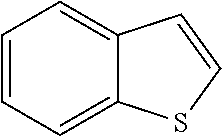
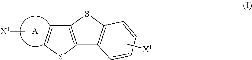
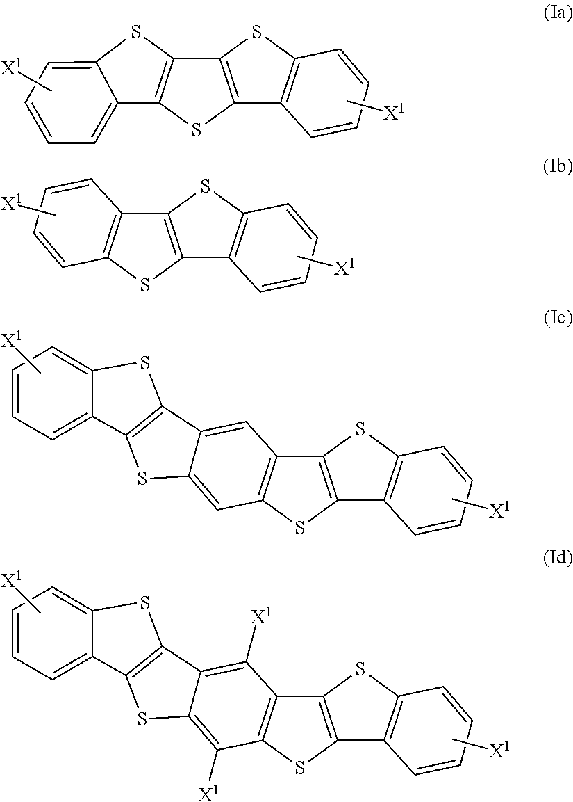
Solution for a semiconducting layer of an organic electronic device
a technology of organic electronic devices and semiconductor layers, which is applied in the direction of organic conductors, non-metal conductors, solid-state devices, etc., can solve the problems of poor film forming properties, difficult to obtain repeatable results from solution processed films and limit the performance of small molecule semiconductors in otfts
- Summary
- Abstract
- Description
- Claims
- Application Information
AI Technical Summary
Benefits of technology
Problems solved by technology
Method used
Image

Examples
example 1
[0133]A mixture of LP-8:F8-TFB in a solution comprising tetrahydronaphthalin and 4-methylanisole was used to form a film. As a result, an improved semiconductor compound morphology of the film is obtained, as illustrated by the cross-polarised optical microscope image of FIG. 5. As is evident therefrom, the coffee stain effect is greatly reduced, although still visible the edges.
[0134]As may be further seen from FIG. 5, the whole surface of the printed pattern is covered with relatively large semiconductor compound crystals, as is shown by the bright vs. dark areas in the cross-polarised optical micrograph. The central region (i.e. transistor channel) advantageously is richer in the amount of small-molecule semiconductor material, while the edge is mainly polymer based.
[0135]The semiconductor compound crystals preferentially orient from the edge of the pattern towards the central region of the printed features. This is attributed to the drying kinetics of the film from the edge, i.e...
PUM
| Property | Measurement | Unit |
|---|---|---|
| weight percent | aaaaa | aaaaa |
| weight percent | aaaaa | aaaaa |
| polydispersity | aaaaa | aaaaa |
Abstract
Description
Claims
Application Information