

Semiconductor device or memory device and driving method thereof
a memory device and semiconductor technology, applied in semiconductor devices, solid-state devices, instruments, etc., can solve the problems of inability to write or erase data at high speed, and the removal of electric charge takes a relatively long time, so as to achieve high reliability, low power consumption, and high-integration of semiconductor devices
- Summary
- Abstract
- Description
- Claims
- Application Information
AI Technical Summary
Benefits of technology
Problems solved by technology
Method used
Image

Examples
embodiment 1
[0039]In this embodiment, an example of a semiconductor device having a function of a memory device is described using drawings.
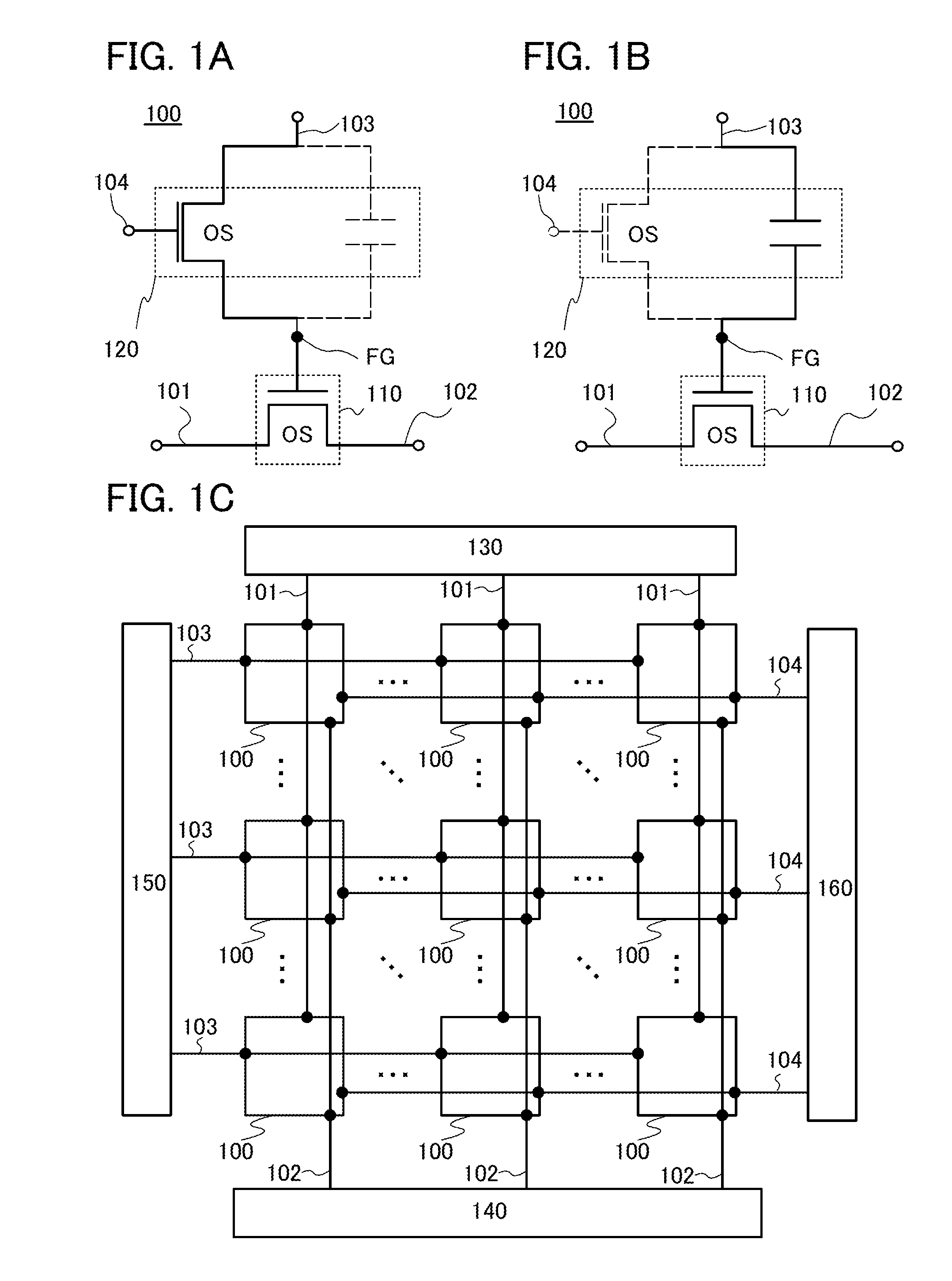
[0040]FIGS. 1A and 1B are circuit diagrams of a semiconductor device (memory device) of one embodiment of the present invention which can hold stored data even when power is not supplied and which has a substantially unlimited number of write cycles.
[0041]A memory cell 100 in FIGS. 1A and 1B includes a first transistor 110 and a second transistor 120. A gate electrode of the first transistor 110 is connected to one of a source electrode and a drain electrode of the second transistor 120. One of a source electrode and a drain electrode of the first transistor 110 is connected to a first wiring 101. The other of the source electrode and the drain electrode of the first transistor 110 is connected to a second wiring 102. The other of the source electrode and the drain electrode of the second transistor 120 is connected to a third wiring 103. A gate electrode o...
embodiment 2
[0087]In this embodiment, a method of manufacturing the semiconductor device described in Embodiment 1 is described with reference to FIGS. 3A to 3C, FIGS. 4A to 4C, FIGS. 5A and 5B, FIGS. 6A and 6B, FIGS. 7A and 7B, and FIGS. 8A and 8B.
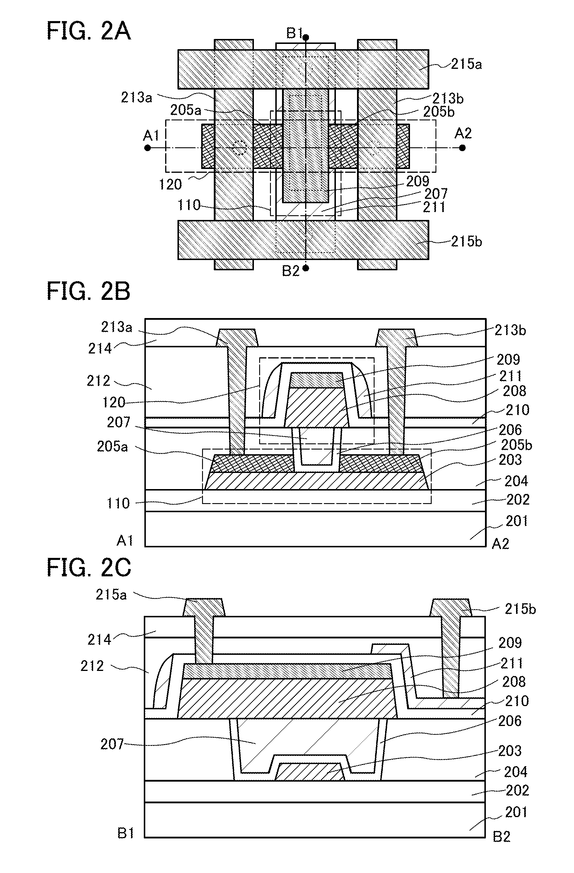
[0088]For the substrate 201, a glass substrate, a ceramic substrate, a quartz substrate, a sapphire substrate, or the like can be used. Alternatively, a single crystal semiconductor substrate or a polycrystalline semiconductor substrate made of silicon, silicon carbide, or the like, a compound semiconductor substrate made of silicon germanium, a silicon-on-insulator (SOI) substrate, or the like can be used. Any of these substrates further provided with a semiconductor element thereover may be used.
[0089]The insulating film 202 is formed over the substrate 201. The insulating film 202 can be formed by a plasma CVD method, a sputtering method, or the like using an oxide insulating film of aluminum oxide, magnesium oxide, silicon oxide, silicon oxynitri...
embodiment 3
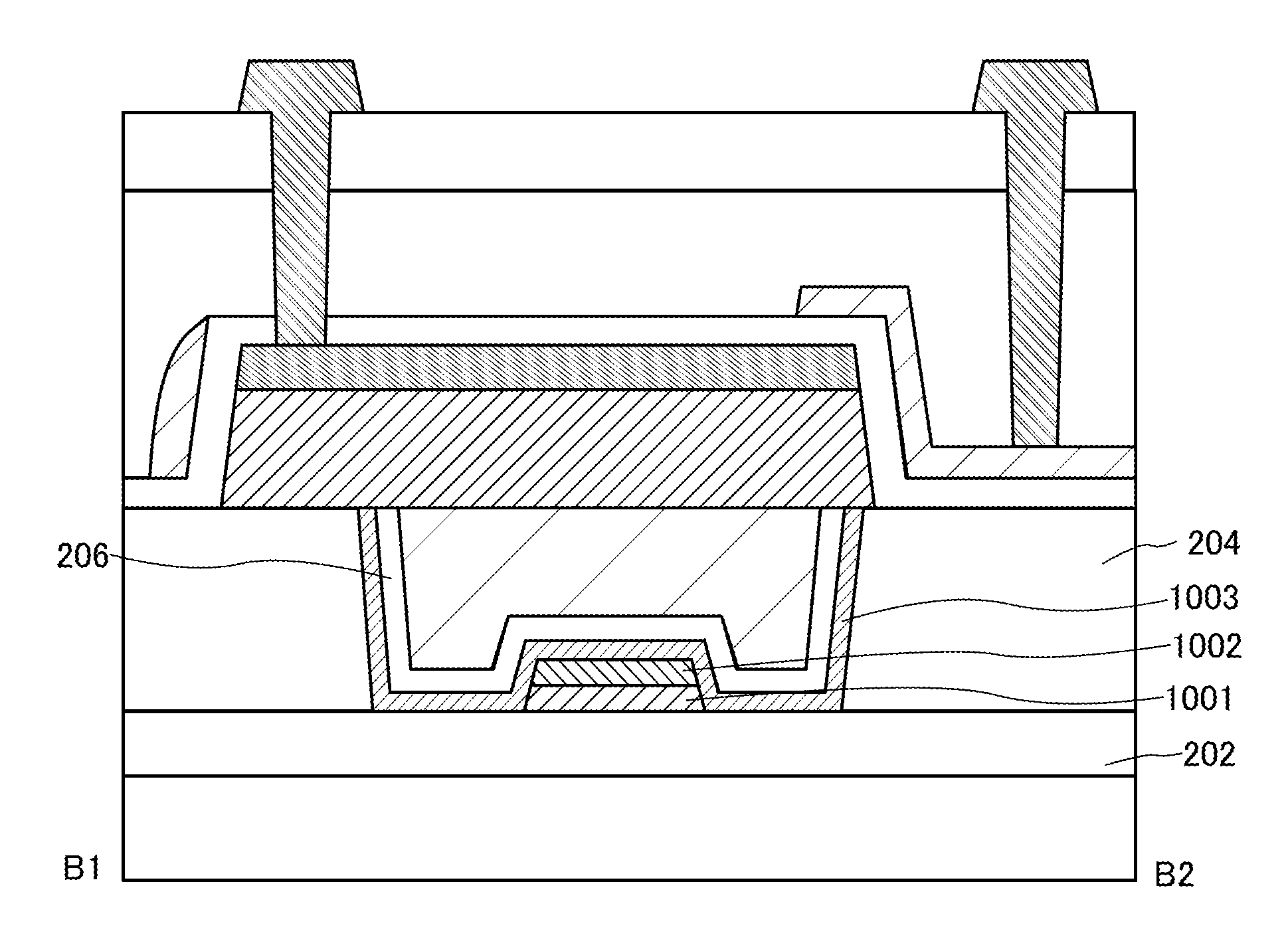
[0141]In this embodiment, a semiconductor device which has a structure different from that of the semiconductor device of Embodiment 1 is described with reference to FIGS. 9A and 9B. FIG. 9A is a cross-sectional view in the channel length direction and FIG. 9B is a cross-sectional view in the channel width direction.
[0142]A difference from the semiconductor device of Embodiment 1 is that a second gate electrode 721 covers a side surface of an upper layer of the second oxide semiconductor layer 208 with the second gate insulating film 210 interposed therebetween and also covers side and top surfaces of the conductive layer 209 with the second gate insulating film 210 interposed therebetween.
[0143]For the second gate electrode 721, a material similar to the materials described for the second gate electrode 211 can be used.
[0144]This embodiment can be combined with any of the other embodiments in this specification as appropriate.
PUM
 Abstract
Description
Claims
Application Information