Conductive cap for metal-gate transistor

a metal-gate transistor and conductive cap technology, applied in the field of metal-gate transistors, can solve the problems of reducing the performance of an electronic device, increasing the gate resistance, increasing the power consumption, etc., and achieves the reduction of the probability of damage to a substrate, the effect of reducing the diffusion of work function materials, and increasing the gate metal resistan

Active Publication Date: 2016-09-22
QUALCOMM INC
View PDF1 Cites 19 Cited by
  • Summary
  • Abstract
  • Description
  • Claims
  • Application Information

AI Technical Summary

Benefits of technology

[0013]One particular advantage provided by at least one of the disclosed aspects is a reduced likelihood of damage to a substrate that may result from diffusion of interconnect material into a substrate. In the present disclosure, a metal-gate transistor (e.g., an HKMG transistor) may include a conductive cap positioned to substantially inhibit diffusion of interconnect material into the substrate. The cap may allow a high-conductivity material such as copper (Cu) to be used as the interconnect material in order to compensate for increased gate metal resistance that is associated with a reduction of dimensions of a gate metal (e.g., when a channel length is reduced to less than 20 nanometers).
[0014]Another advantage provided by at least one of the disclosed aspects is a reduction of diffusion of work function material (e.g., of one or more work function layers of a metal-gate transistor) that may occur when an interconnect directly overlies the work function material. Diffusion of work function material into the interconnect may result in threshold voltage (Vt) fluctuation. Positioning the cap between the work function material and the interconnect may reduce Vt fluctuation by substantially inhibiting diffusion of the work function material into the interconnect.

Problems solved by technology

As an example, leakage current may increase for a smaller process technology and a smaller gate oxide thickness, resulting in increased power consumption.
Increased gate resistance can reduce performance of an electronic device.
For example, increased gate resistance may be associated with greater power consumption and slower circuit operation.
Boundary areas between various layers of an HKMG transistor may allow for solid-state diffusion of interconnect material into a substrate, potentially resulting in damage to the substrate.
In cases where an interconnect material directly overlies the vertical layers of the HKMG transistor, the boundary areas between the vertical layers may allow for solid-state diffusion of interconnect material into the substrate, potentially causing damage to the substrate.
Further, the cap may substantially inhibit diffusion of work function material into the interconnect that may result in threshold voltage (Vt) fluctuation.
Diffusion of work function material into the interconnect may result in threshold voltage (Vt) fluctuation.

Method used


Image

  • Conductive cap for metal-gate transistor
  • Conductive cap for metal-gate transistor
  • Conductive cap for metal-gate transistor

Examples


Embodiment Construction

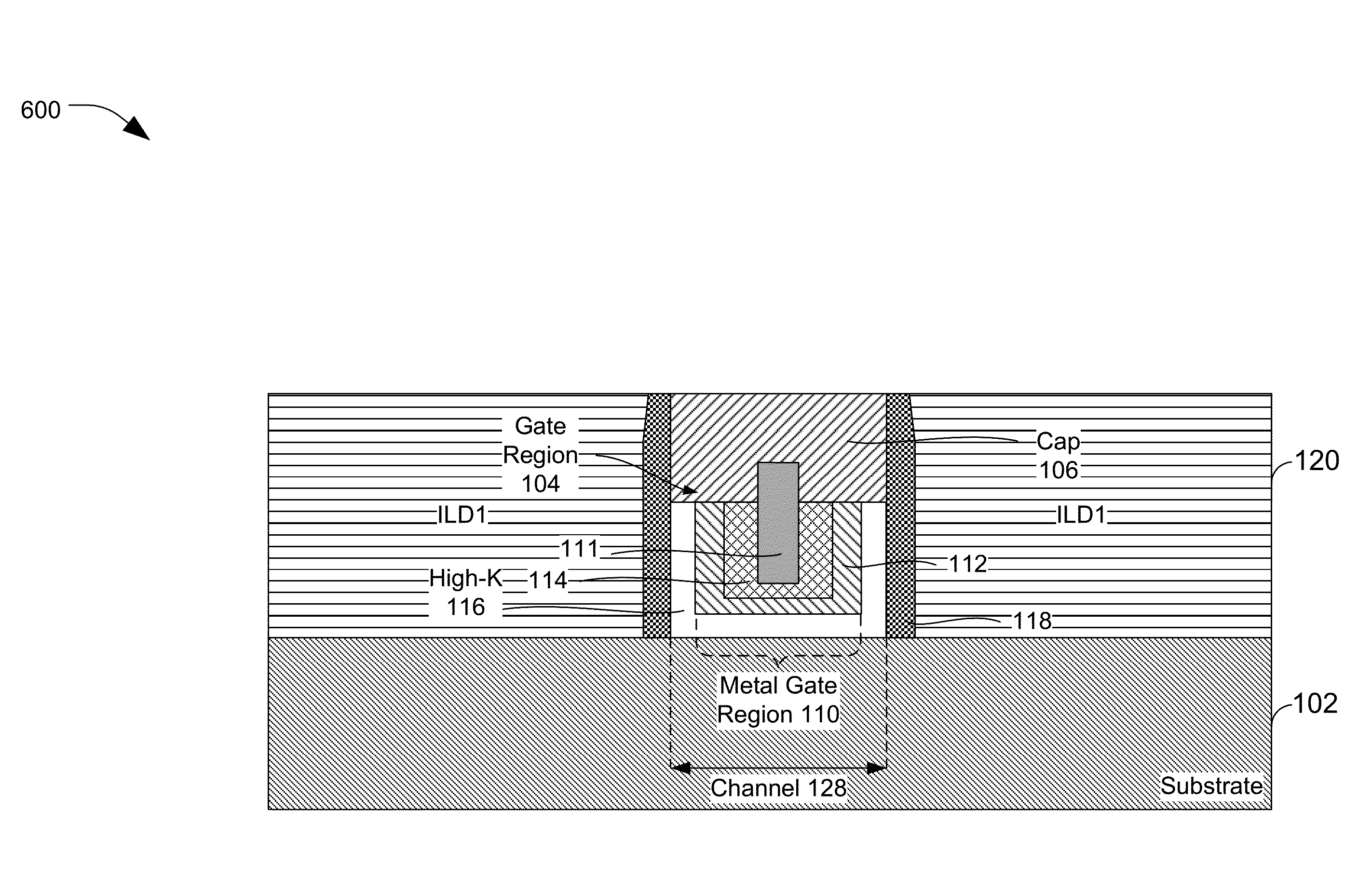
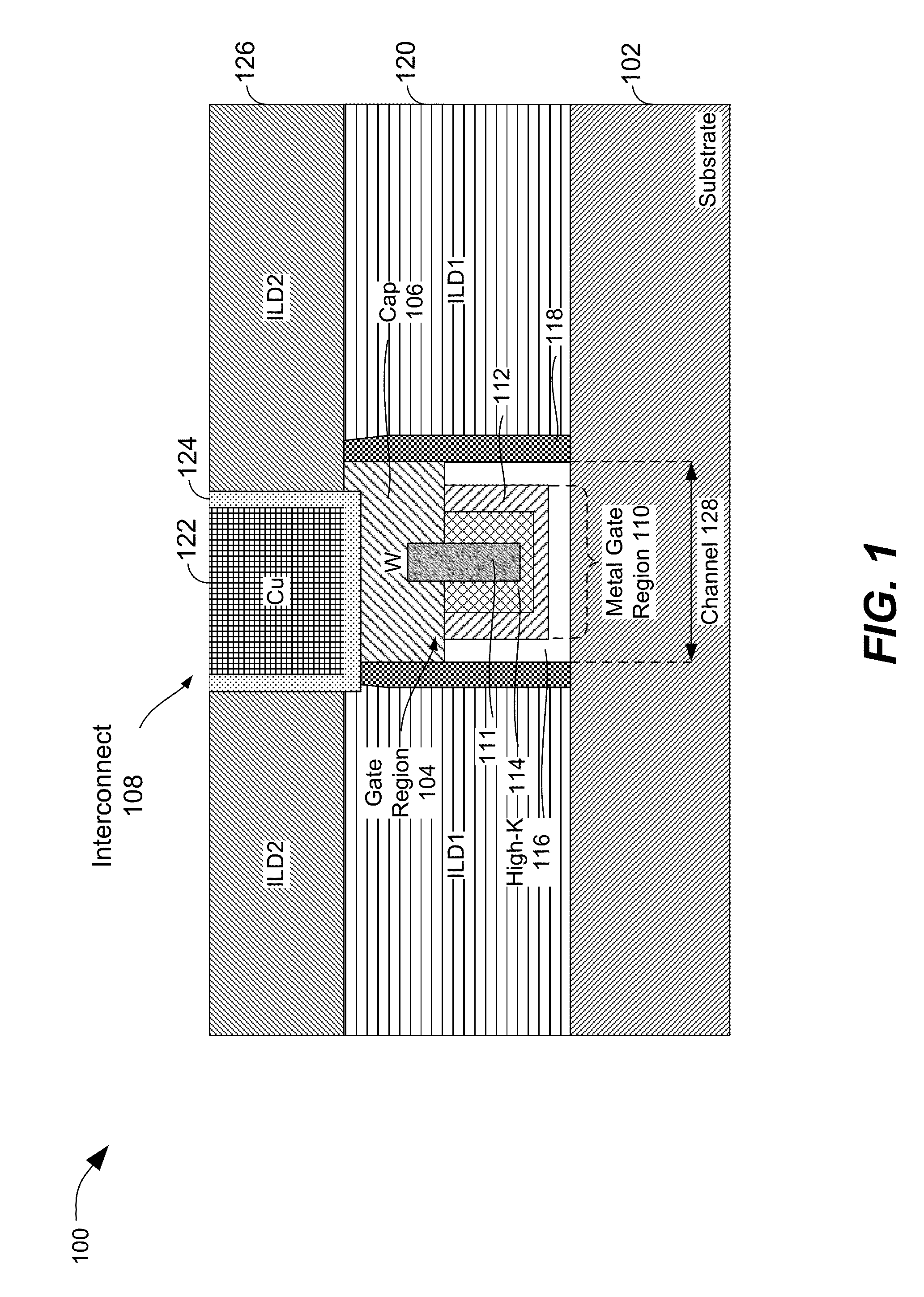
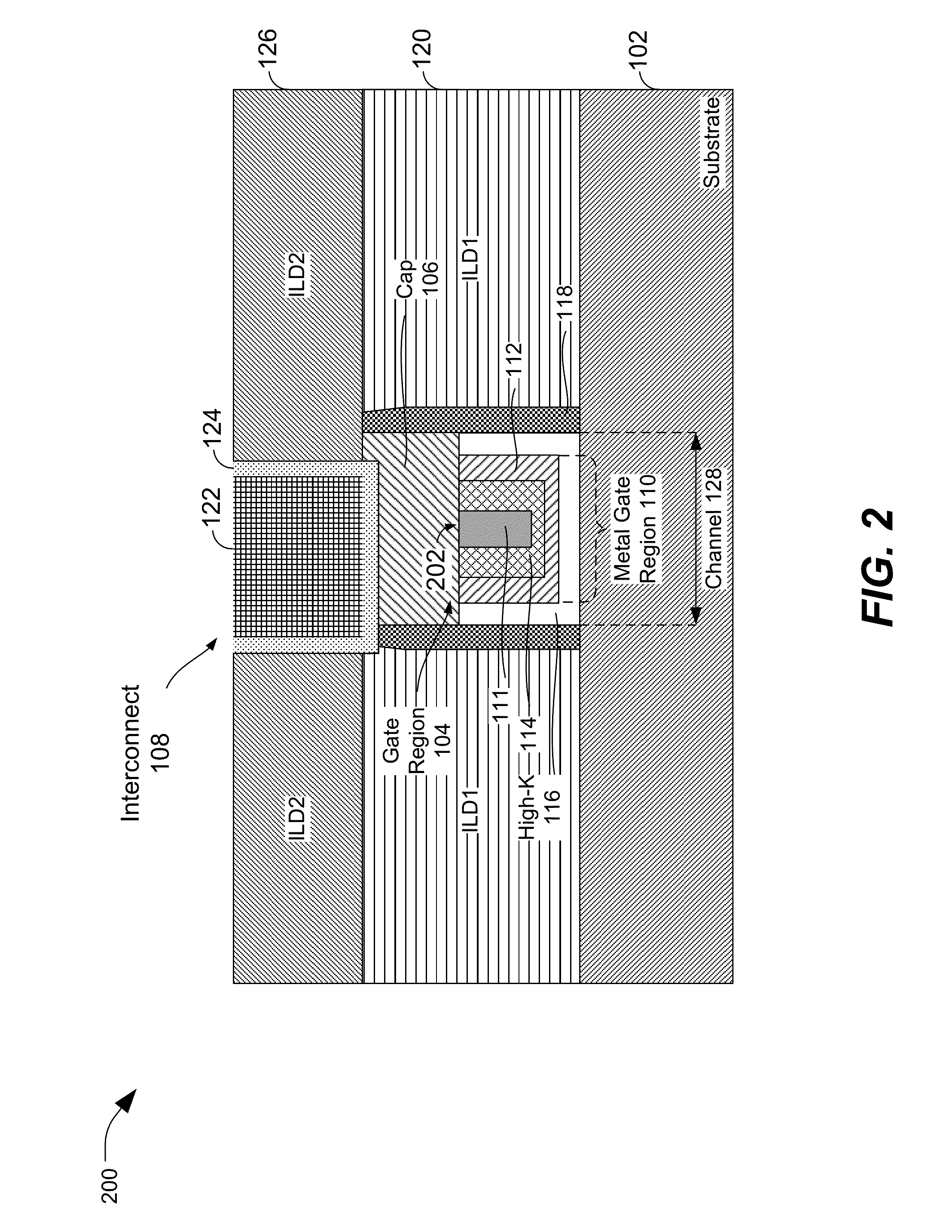
[0036]FIG. 1, as described herein, illustrates a side view of a first instance of a structure 100. FIG. 2, as described herein, illustrates a side view of a second instance of a structure 200. FIG. 3, as described herein, illustrates a side view of a structure 300 during a particular stage of a process of fabricating an electronic device (e.g., a semiconductor device, an integrated circuit device, or another electronic device) that includes the structure 100 of FIG. 1 or the structure 200 of FIG. 2. FIGS. 4-10, as described herein, illustrate side views of structures as formed during multiple stages of a process of fabricating an electronic device that includes the structure 100 of FIG. 1. FIGS. 11-17, as described herein, illustrate side views of structures as formed during multiple stages of a process of fabricating an electronic device that includes the structure 200 of FIG. 2.

[0037]Referring to FIG. 1, a diagram of a side view of a structure as formed during a process of fabrica...


PUM


Abstract

A semiconductor device includes a gate region, a conductive cap, and an interconnect. The gate region (e.g., a metal-gate transistor) includes a metal gate region and a high dielectric constant (high-K) gate dielectric region. The conductive cap is disposed on a surface of the metal gate region and on a surface of the high-K gate dielectric region, and the interconnect is disposed on the conductive cap. The conductive cap includes a conductive material that electrically connects the gate region to the interconnect.

Description

I. FIELD[0001]The present disclosure is generally related to metal-gate transistors and more particularly to high dielectric constant (high-K) metal-gate (HKMG) transistors.II. DESCRIPTION OF RELATED ART[0002]Advances in technology have resulted in smaller and more powerful computing devices. For example, a variety of portable personal computing devices, including wireless telephones such as mobile and smart phones, tablets and laptop computers, are small, lightweight, and easily carried by users. These computing devices can communicate voice and data packets over wireless networks. Further, many such computing devices incorporate additional functionality such as a digital still camera, a digital video camera, a digital recorder, and an audio file player. Also, such computing devices can process executable instructions, including software applications, such as a web browser application, that can be used to access the Internet. As such, these computing devices can include significant...

Claims


Application Information

Patent Timeline
Patent Type & Authority Applications(United States)
IPC IPC(8): H01L29/49H01L29/06H01L29/66H01L21/28H01L21/768H01L21/3213H01L23/528H01L23/532H01L29/51H01L29/78
CPCH01L29/4958H01L29/517H01L29/0649H01L29/66568H01L29/78H01L21/7684H01L21/32133H01L23/528H01L23/53238H01L21/28079H01L21/76897H01L21/28114H01L21/28247H01L21/76877H01L21/823475H01L29/42376H01L29/4966
Inventor YANG, HAININGSONG, STANLEY SEUNGCHUL
Owner QUALCOMM INC
Why Eureka
Try Eureka