Method and device for polymerizing a composition comprising hydridosilanes and subsequently using the polymers to produce silicon-containing layers

Active Publication Date: 2016-10-13
FORSCHUNGSZENTRUM JILICH GMBH
View PDF2 Cites 15 Cited by
  • Summary
  • Abstract
  • Description
  • Claims
  • Application Information

AI Technical Summary

Problems solved by technology

The drawback of photochemical methods known from the prior art for producing coating solutions (precursors) for silicon layers is that they are very time- and labor-intensive.
Photopolymerization is a very time-consuming method.
Irradiations typically last between 10 and 120 minutes [2] [3] or up to 840 minutes [DE 10 2010 041 842 A1], and the use of UV irradiation incurs additional procurement costs, and safety measures may need to be taken.
The method has disadvantages when silicon layers for optoelectronic applications are produced since it requires the use of expensive vacuum technology and a modified scanning electron microscope (SEM).
Here, the method has the disadvantage that the production of intrinsic silicon layers is made more difficult due to the doping property of Ga.
This method has the disadvantage that it is energy-intensive and that, due to the heating process or the residual thermal energy of the solution, the polymerization cannot be immediately initiated (due to the heating process) or immediately terminated (due to the cooling process) without additional work steps.
The disadvantages of all of the above-mentioned methods for producing coating solutions for silicon layers are the time-intensive temperature and

Method used


Image

  • Method and device for polymerizing a composition comprising hydridosilanes and subsequently using the polymers to produce silicon-containing layers
  • Method and device for polymerizing a composition comprising hydridosilanes and subsequently using the polymers to produce silicon-containing layers
  • Method and device for polymerizing a composition comprising hydridosilanes and subsequently using the polymers to produce silicon-containing layers

Examples


example 2

Polymerization of a Composition by Way of a Sonotrode

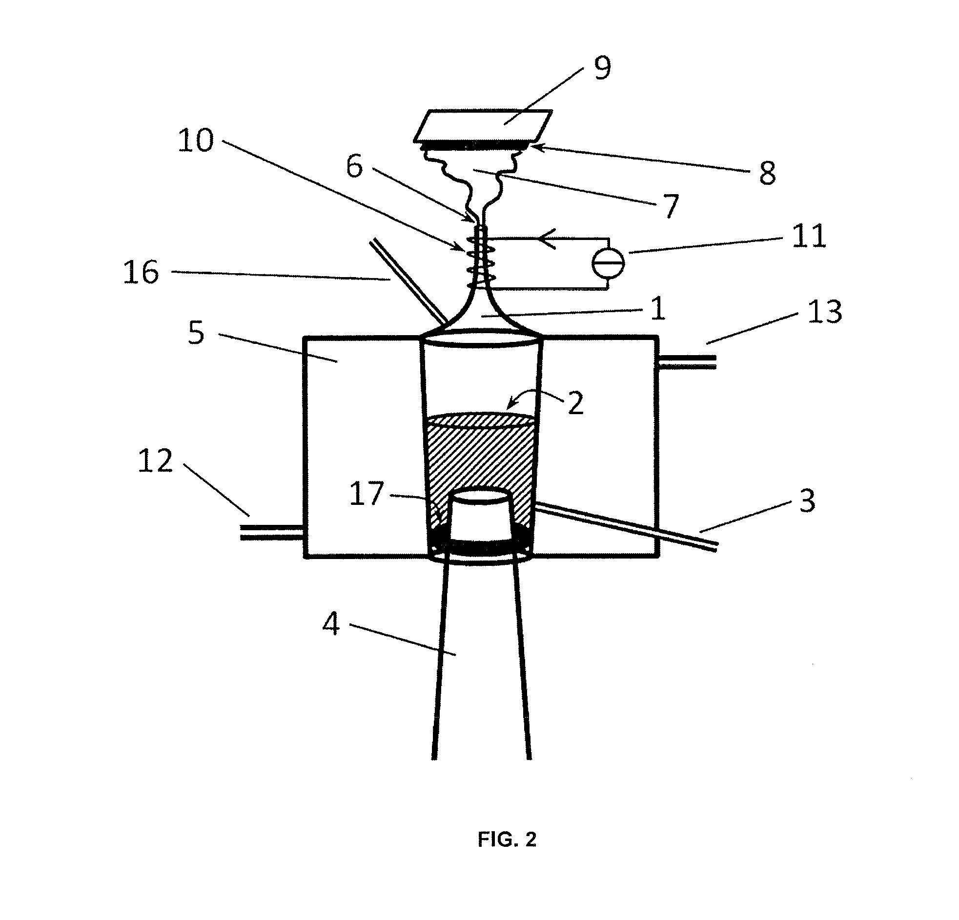
[0079]A composition having a volume of 0.8 ml, including 5.6% by weight cyclopentasilane in cyclooctane, was placed in the reaction vessel (1) and sonified at a process temperature of less than 65° C. for approximately 50 minutes using an ultrasonic frequency of approximately 25 kilohertz (kHz), and caused to polymerize by way of acoustic cavitation until a slight turbidity was detectable. A sonotrode and the device according to FIG. 2 were used for this purpose. The opening (6) of the device was closed for the polymerization process. The mean molar mass Mw of the polymers produced according to the invention, ascertained by way of gel permeation chromatography (GPC), was 1430 g / mol.

example 3

Coating a Substrate with Polymers by Way of Spin Coating

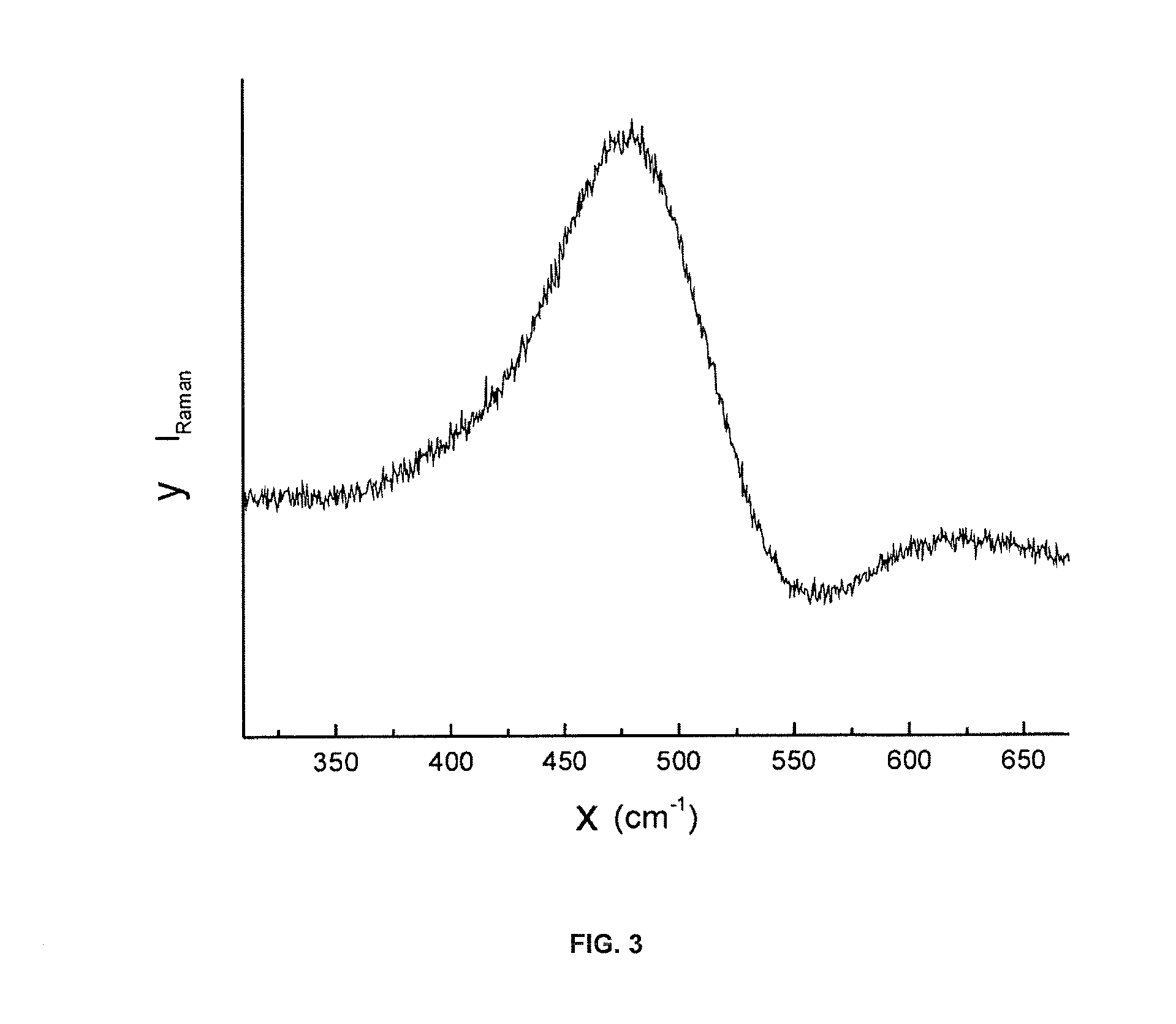
[0080]The reaction products from Example 1, containing higher hydridosilanes, were subsequently removed from the device via the feed / discharge pipe (3) and applied to a glass substrate by way of spin coating, which is known from the prior art, at a rotation speed of 2000 revolutions per minute (rpm) for 45 seconds. Following conversion on a heating plate at approximately 350° C., the layer had a thickness of 25 nm. FIG. 3 shows a Raman spectrum of this silicon layer, in which it is apparent that the layer has a completely amorphous character due to the transverse optical (TO) Raman scattering peak at an approximate wavenumber of 480 cm−1.

[0081]The reaction products from Example 2 were likewise applied to a glass substrate by way of spin coating at 2000 rpm for 50 seconds and subsequently converted at approximately 350° C. The thickness of the resulting amorphous layer was 38 nm.

example 4

Coating a Substrate with Nanoparticles with the Aid of Nanoparticle Aerosol Droplets

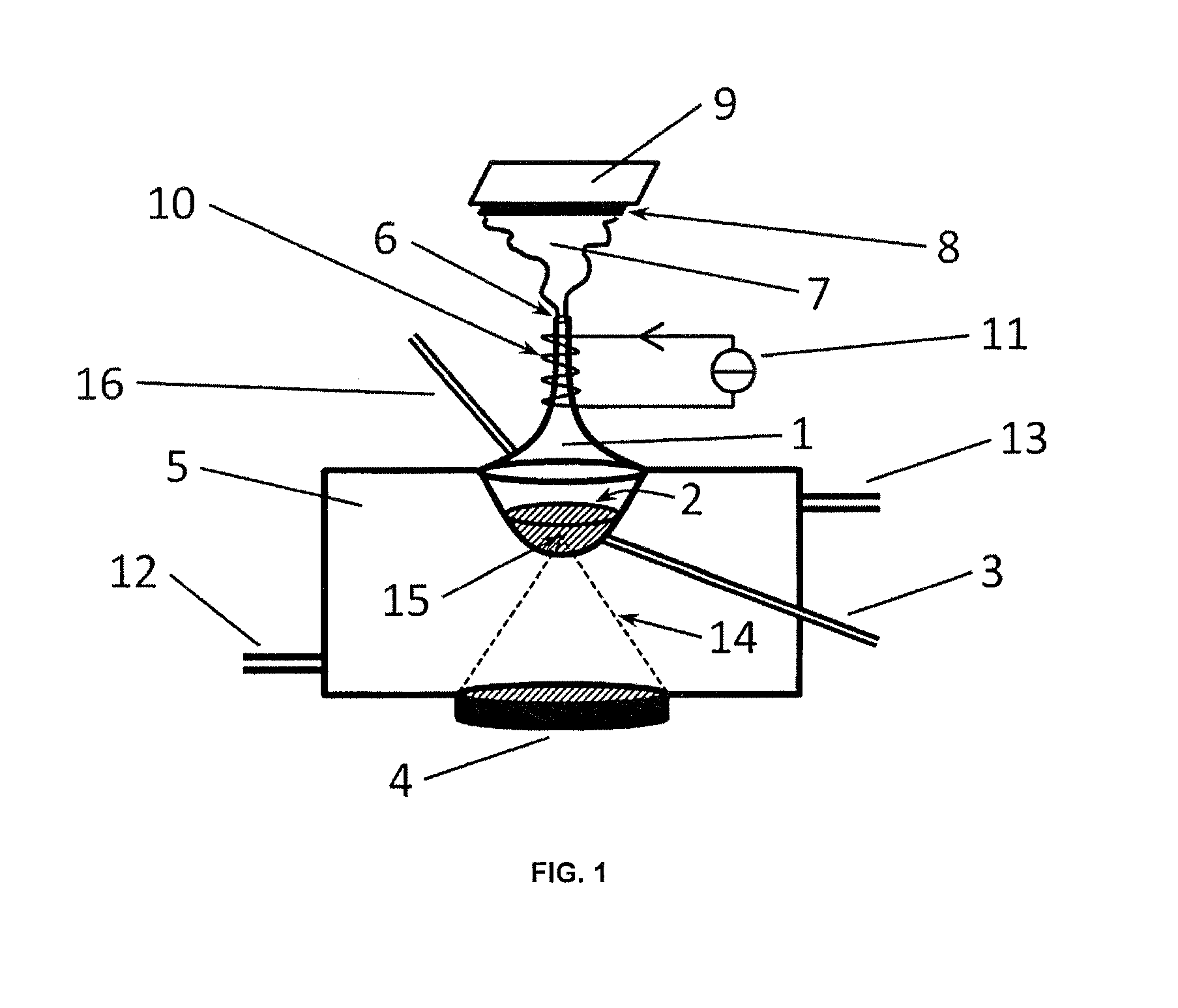
[0082]A composition containing Fe2O3 nanoparticles having a diameter of approximately 40 nm was dispersed in an organic / inorganic solvent mixture, placed in the reaction vessel (1), and subsequently converted into nanoparticle aerosol droplets by way of acoustic cavitation and / or capillary waves, and applied to a structured substrate surface. A piezoceramic and the device according to FIG. 1 were used for this purpose. The coating of the substrate surface with the nanoparticle aerosol droplets was carried out at room temperature (approximately 23° C.) and within a coating time of approximately 3 seconds. The acoustic cavitation and capillary wave formation triggered by the piezoceramic resulted in the formation of nanoparticle aerosol droplets, which migrated through the opening (6) of the reaction vessel (1) and were deposited on the substrate (8), which is disposed opposite the opening (6). As is a...


PUM

PropertyMeasurementUnit
Temperatureaaaaaaaaaa

Abstract

A method for polymerizing a composition including hydridosilanes and subsequently using the polymers to produce silicon containing layers, comprising the following steps: a) providing a substrate; b) providing a composition including at least one hydridosilane that is dissolved in at least one organic and/or inorganic solvent, or including at least one hydridosilane that is already present in liquid form without solvent, wherein the hydridosilanes comprise at least one linear and/or one branched hydridosilane of the general formula SinH2n+2, where n≧3, and/or a cyclic hydridosilane of the general formula SinH2n, where n≧3; c) polymerizing the composition from step b) by way of acoustic cavitation; and d) coating the surface of the substrate with reaction products from step c). A device for polymerizing a composition including hydridosilanes and subsequently using the polymers to produce silicon containing layers, comprising at least one reaction vessel (1) containing a composition that includes at least one hydridosilane that is dissolved in at least one organic and/or inorganic solvent, or at least one hydridosilane that is already present in liquid form without solvent, wherein the hydridosilanes comprise at least one linear and/or branched hydridosilane of the general formula SinH2n+2, where n≧3, and/or a cyclic hydridosilane of the general formula SinH2n, where n≧3, and/or containing the abovementioned hydridosilane solution or the pure liquid hydridosilane, to which at least monosilane and/or disilane and/or boron containing dopant and/or phosphorus containing dopant and/or a noble gas from the group Ar, He and/or nanoparticles and/or a polymerization initiator and/or a catalyst and/or surface tension modifying agents can be added, and an ultrasound source and/or a sound transducer (4) for generating acoustic cavitation and/or capillary waves, wherein the reaction vessel (1) has at least one closable opening (6), the substrate (8) to be coated is disposed opposite the opening (6), and the substrate (8) comprises a heating source (9) on the surface that faces away from the coating surface.

Description

[0001]The invention relates to a method for polymerizing a composition comprising hydridosilanes and subsequently using the polymers to produce silicon-containing layers. The invention further relates to a device that makes the aforementioned method possible, to layers produced by way of the method, and to the use thereof to produce semiconducting or insulating thin layers with or without nanoparticles embedded therein.PRIOR ART[0002]To produce solar cells, semiconductor layers having differing dopings are required, which include at least one Schottky or p-n junction. As is known from the prior art (WO 2011 / 061106 A2), a pin junction can be generated by depositing an amorphous layer sequence, containing higher silanes, among other things, on a suitable substrate using liquid phase deposition, the junction acting as a solar cell with suitable front and rear contacts. In the production of thin-film solar cells based on p-i-n junctions, the individual doping layers are doped as an n-si...

Claims


Application Information

Patent Timeline
IPC IPC(8): C09D183/16C23C18/12H01L31/18C08G77/06C08G77/60
CPCC09D183/16C08G77/06C23C18/122H01L31/1804C08G77/60
Inventor CADIZ BEDINI, ANDREW PAOLO
Owner FORSCHUNGSZENTRUM JILICH GMBH
Why Eureka
Try Eureka