Magnetoresistive Random Access Memory Cell

a random access and memory cell technology, applied in the direction of magnetic field-controlled resistors, digital storage, instruments, etc., can solve the problems of slow write, flash memory has limited endurance of writing cycle, and information loss

Inactive Publication Date: 2016-10-13
GE YI +1
View PDF0 Cites 74 Cited by
  • Summary
  • Abstract
  • Description
  • Claims
  • Application Information

AI Technical Summary

Benefits of technology

[0016]For both cases, a particular structure, which provides a lateral magnetic bias field, is placed either in the stack or close to the stack to assist the switching of the magnetic storage layer and to low the critical switching current (or current density).
[0018]For the Case II, the complementary magnetic layer and its distance from the storage layer is engineered in such a way that the magnetic field emitting from the storage layer is capable of leaving a matched magnetic footprint within the magnetic layer. The interaction between the magnetic footprint and the magnetic storage layer leads a huge benefits, particularly for in-plane TMR stack based MRAM cell designs.

Problems solved by technology

Nevertheless, both DRAM and SRAM are volatile memory, which means they lost the information stored once the power is removed.
However, flash memory has limited endurances of writing cycle and slow write though the read is relatively faster.
It has poor scalability beyond 65 nm because the write current in the write line needs to continue increase to ensure reliable switching the magnetization of the magnetic storage layer because of the fact that the smaller the physical dimension of the storage cell, the higher the magnetic coercivity it normally has for the same material.
Nevertheless, the only commercially available MRAM so far is based on this conventional writing scheme.
Despite of intensive efforts and investment, even with the early demonstrated by Sony in late 2005, no commercial products are available on the market so far.
One of the biggest challenges of STT-RAM is its reliability, which depends largely on the value and statistical distribution of the critical current density needed to flip the magnetic storage layers within every patterned TMR stack used in the MRAM memory structures.
To allow such a large current density to flow through the dielectric barrier layer such as AlOx and MgO in the TMR stack, the thickness of the barrier has to be relatively thin for writing energy reduction; however such a thin barrier not only limits the magnetoresist (MR) ratio value but also causes potential risk of the barrier breakdown.
However, when SOT effect is used to design magnetic memory cell, there is still a lot of challenges.
Unfortunately, as the size of the memory cell (i.e. the footprint of the storage layer: S) is reduced, with a thin storage layer (with thickness of t), the thermal stability of the storage layer is in serious doubt because of the thermal stability factor KV / kBT being proportion to the total magnetic volume (V=S*t) of storage layer (K is magnetic anisotropy of storage layer, S is the cross section of storage layer, t is the thickness of storage layer, kB is the Boltzmann, T is the temperature in absolute temperature unit).
For memory cell design based on perpendicular storage layer (or perpendicular TMR stack), even without considering the magnitude of current density for the SOT effect, there are some practical challenges.
However, the in-plane TMR stack based MRAM cell design, in general, has its own unresolved issue, i.e., the magnetic interaction between the adjacent cells due to fringe magnetic field from the storage layers causing instability and wide spread of the switching current density variation.
Moreover, the thicker the storage layer, the worse the inter-cell magnetic cross-talk as well as the larger the critical current density needed for SOT to flip the storage layer.

Method used


Image

  • Magnetoresistive Random Access Memory Cell
  • Magnetoresistive Random Access Memory Cell
  • Magnetoresistive Random Access Memory Cell

Examples


Embodiment Construction

[0028]The following description is provided in the context of particular designs, applications and the details, to enable any person skilled in the art to make and use the invention. However, for those skilled in the art, it is apparent that various modifications to the embodiments shown can be practiced with the generic principles defined here, and without departing the spirit and scope of this invention. Thus, the present invention is not intended to be limited to the embodiments shown, but is to be accorded the widest scope consistent with the principles, features and teachings disclosed here.

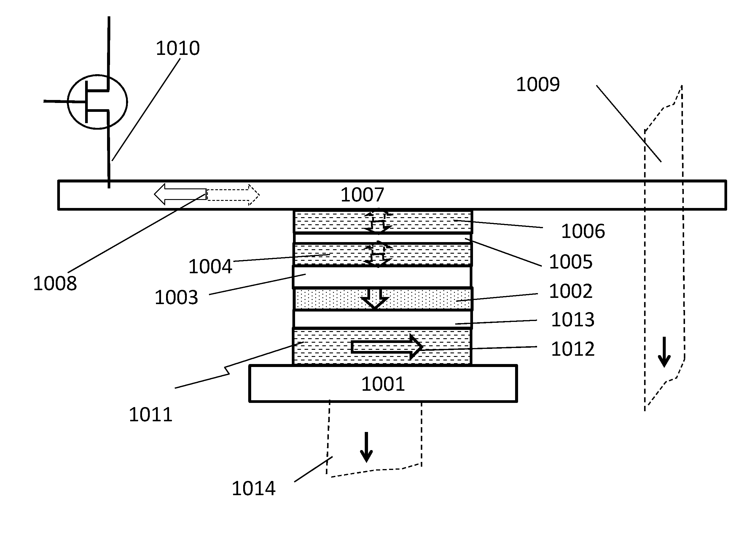
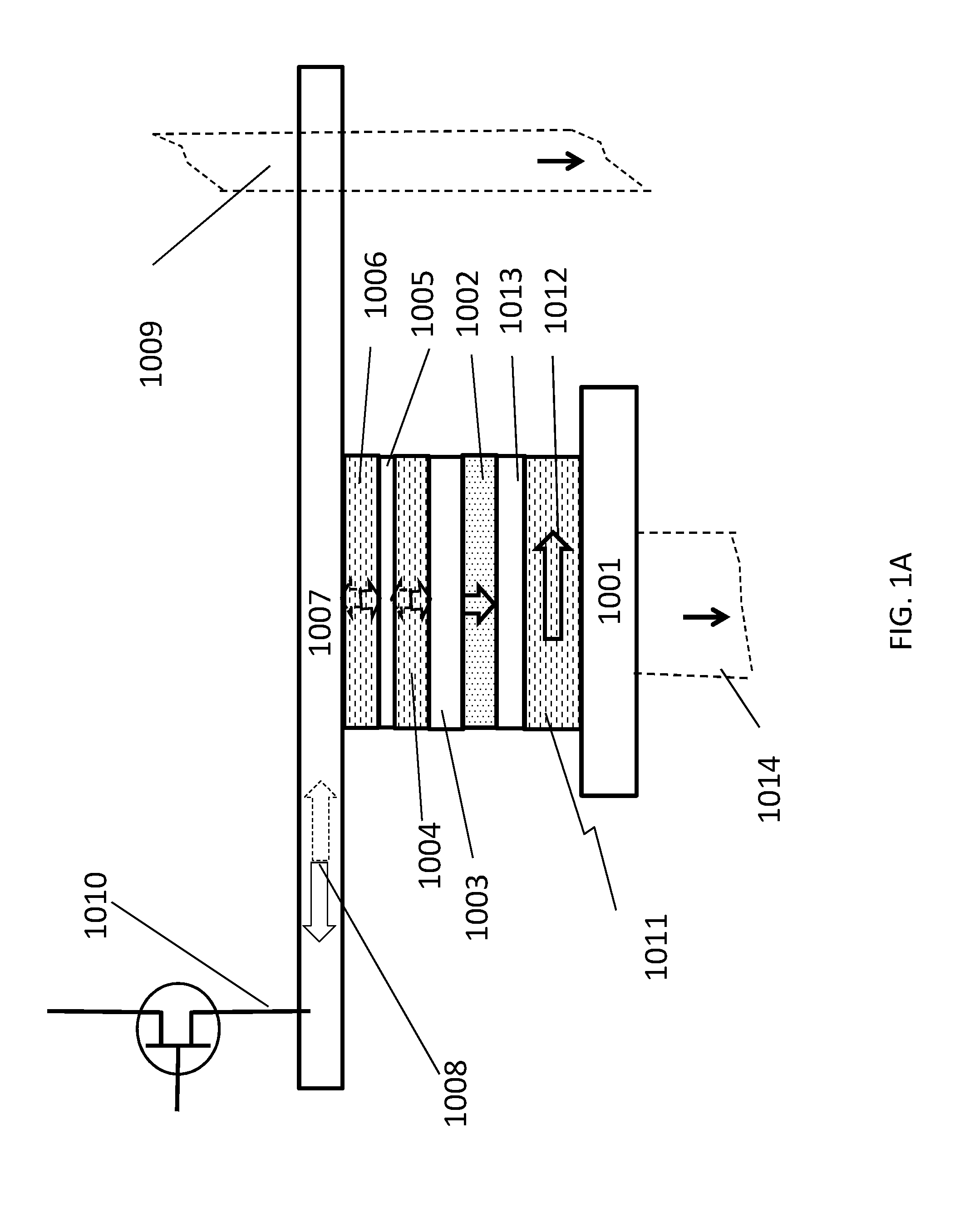
[0029]FIG. 1A illustrates one embodiment of the proposed SOT-MRAM cells based on perpendicular TMR stack locating at the bottom of the cell structure, together with an in-stack magnet providing a magnetic field bias to storage layer along the switching current direction. The in-stack bias magnet is just an optional, which helps to low the switching / write current of the cell. In the following...


PUM


Abstract

A novel three-terminal MRAM memory cell with an independent sensing and writing paths, a composite data storage layer together with a bias magnetic field for the data storage layer has been invented. The interaction between the magnetic layers within the composite data storage layer is either via Ruderman-Kittel-Kasuya-Yosida (RKKY) coupling, or magnetostatic coupling, or orange peel coupling, or even a direct ferromagnetic coupling. The design improves magnetic and thermal stability of the cell, thus capable for higher area density.

Description

RELATED APPLICATIONS[0001]The present application claims of the priority benefit of U.S. 62 / 108,071—a provisional patent application—directly related. The present application also claims of the priority benefit of two previous applications: firstly, U.S. patent application Ser. No. 13 / 288,860 filed on Nov. 3, 2011 as utility application, published on May 9, 2013 as US2013 / 0114334A1 entitled “MAGNETORESISTIVE RANDOM ACCESS MEMORY CELL WITH INDEPENDENTLY OPERATING READ AND WRITE COMPONENTS”; secondly, U.S. patent application Ser. No. 14 / 506,618 filed on Nov. 4, 2014 as utility application entitled “MAGNETORESISTIVE RANDOM ACCESS MEMORY CELL and 3D MEMORY CELL ARRAY”; which are incorporated herein by reference.FIELD OF INVENTION[0002]The invention is related to magnetoresistive random access memory cell design. Particularly, the so-called spin-orbit torque magnetoresistive random access memory (SOT-MRAM) cell design for improving its thermal and magnetic stability.BACKGROUND ART[0003]D...

Claims


Application Information

Patent Timeline
Patent Type & Authority Applications(United States)
IPC IPC(8): H01L43/02H01L43/08G11C11/16
CPCH01L43/02H01L43/08G11C11/161G11C11/1673G11C11/1675G11C11/18H10N50/10H10N50/85
Inventor YI, GELI, ZHANJIE
Owner GE YI
Why Eureka
Try Eureka