Method and device for cutting wafers

a technology of wafers and cutting tools, applied in the field of methods and devices, can solve problems such as reducing productivity, and achieve the effect of improving productivity

Active Publication Date: 2016-10-27
ASMPT SINGAPORE PTE LTD
View PDF3 Cites 14 Cited by
  • Summary
  • Abstract
  • Description
  • Claims
  • Application Information

AI Technical Summary

Benefits of technology

[0011]An objective of the present invention is to seek to provide a laser cutting method that is capable of

Problems solved by technology

Although the above-described laser cutting method has proven to give results with very good quality, it has a drawback that cutting a single groove involves three cutting actions performed in two subsequent cutting steps, i.e. a first step comprising the two scribing actions of scribing two trenches with two low power beams and a second step comprising the cutting action of cutting a central fissure with one or more high

Method used


Image

  • Method and device for cutting wafers
  • Method and device for cutting wafers
  • Method and device for cutting wafers

Examples


Embodiment Construction

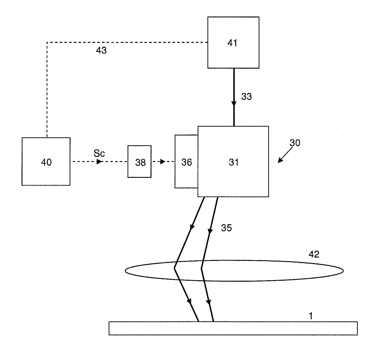
[0024]For convenience, the term “cut” is hereinafter used generically to include scribing (cutting that does not penetrate the full depth of a target work piece) and dicing (cutting through the depth of the target work piece). Moreover, the term “fissure” is hereinafter used generically to include different types of cuts such as a groove formed by scribing or a full cut formed by dicing a target work piece.

[0025]An aspect of the present invention involves a controllable beam deflector. A controllable beam deflector is a device capable of changing the direction of an optical beam and of precisely controlling its deflection angle, typically within a certain deflection range. Controllable beam deflectors are known per se, for instance from U.S. Pat. No. 4,028,636, therefore a description and explanation will be kept brief.

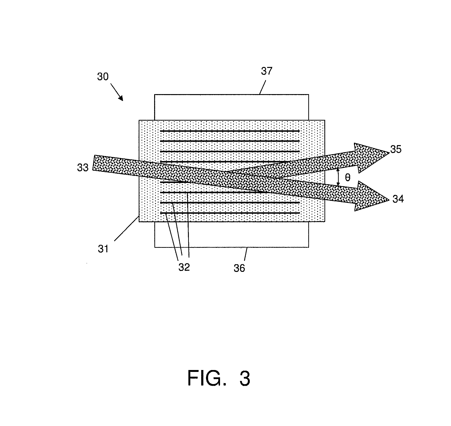
[0026]FIG. 3 schematically shows the setup and operation of an acousto-optical deflector 30, hereinafter abbreviated as AOD. The AOD 30 comprises an optical crystal 3...


PUM

PropertyMeasurementUnit
Angleaaaaaaaaaa
Widthaaaaaaaaaa
Frequencyaaaaaaaaaa

Abstract

A method is described of radiatively cutting a wafer, the method comprising the steps of low power cutting of two trenches followed by high power cutting of a fissure. A single pulsed radiation beam is split into a first pulsed radiation beam for cutting at least one of the trenches and a second pulsed radiation beam for cutting the fissure. When cutting a fissure on the wafer in a cutting direction along a cutting street, the first and second radiation beams are directed simultaneously with the first radiation beam leading and the second radiation beam trailing. For cutting a fissure in the opposite cutting direction, a third pulsed radiation beam for trenching is split from said single pulsed radiation beam.

Description

FIELD OF THE INVENTION[0001]The present invention relates in general to the field of semiconductor manufacture.BACKGROUND OF THE INVENTION[0002]Miniaturization of electronic components has led to various improvements in semiconductor technology to make electronic components ever-smaller. Such components may include simple components such as diodes, up to complex components such as integrated circuits. Apart from electronic components, mechanical components can also be manufactured using the same technology.[0003]In the art of semiconductor technology, it is commonly known that a wafer of semiconductor material, typically silicon, is processed to form the components in a surface area of the wafer. The wafer is macroscopic, having a diameter ranging in the order of 20-300 mm, while the components are microscopic, typically having a size in the micrometer range. Each component is made in a small wafer portion, with the various wafer portions being located at a small distance from each ...

Claims


Application Information

Patent Timeline
IPC IPC(8): H01L21/78B23K26/082H01L21/67B23K26/402H01L21/268B23K26/067B23K26/364
CPCH01L21/78B23K26/0676B23K26/082B23K2203/56B23K26/402H01L21/268H01L21/67115B23K26/364H01L21/67092B23K26/38B23K26/0622B23K2101/40H01L21/76H01L21/02354
Inventor VAN DER STAM, KAREL MAYKEL RICHARD
Owner ASMPT SINGAPORE PTE LTD
Why Eureka
Try Eureka