Device for manufacturing integrated thin film solar cell

a technology of solar cells and solar cells, which is applied in the direction of basic electric elements, electrical apparatus, and semiconductor devices, can solve the problems of reducing the effective area of electric power generated by the entire integrated thin film solar cell, the inability to continuously perform the deposition process in vacuum, and the thickness of silicon substrate, etc., to achieve the effect of maximizing the effective area, maximizing the electric power production, and high efficiency

Inactive Publication Date: 2016-11-10
KOREA ADVANCED INST OF SCI & TECH
View PDF5 Cites 6 Cited by
  • Summary
  • Abstract
  • Description
  • Claims
  • Application Information

AI Technical Summary

Benefits of technology

[0020]According to the embodiment of the present invention described above, it is possible to manufacture an integrated thin film solar cell which maximizes the effective area by performing repeatedly or continuously only a deposition process in a plurality of vacuum process chambers or by performing repeatedly or continuously the deposition process and an etching process in the plurality of vacuum process chambers, thereby maximizing the electric power production.
[0021]According to the embodiment of the present invention, it is possible to manufacture the integrated thin film solar cell with a multi junction structure as well as a single-junction structure in the plurality of vacuum process chambers.
[0022]According to the embodiment of the present invention, it is possible to manufacture the integrated thin film solar cell which has a high efficiency without breaking the vacuum in order to fundamentally solve a problem that, whenever a substrate on which each thin film has been deposited is exposed to the air so as to perform a laser patterning process, each layer of the solar cell is contaminated by moisture, dust, etc., in the air, so that the interface properties of a device are deteriorated, and thus, the energy conversion efficiency of the device is degraded.
[0023]According to the embodiment of the present invention, it is possible to manufacture the integrated thin film solar cell which has a high efficiency without using laser in order to fundamentally solve a problem that fine holes, i.e., pin holes are formed in the thin film by the dust generated by the laser scribing, so that then a shunt resistance is reduced, and the thin film is thermally damaged by the laser energy, so that the film characteristics are deteriorated and the junction characteristics of the device are deteriorated, and thus, the energy conversion efficiency of the device is degraded.
[0024]According to the embodiment of the present invention, it is possible to manufacture the integrated high efficiency thin film solar cell which has a low manufacturing cost even without a substrate inverter, a substrate cleaner, and several expensive laser apparatuses for the purpose of the countermeasures against the dust.
[0025]According to the embodiment of the present invention, it is possible to manufacture the integrated see-through type thin film solar cell even without using an expensive laser apparatus.

Problems solved by technology

However, since a wafer, i.e., a substrate occupies a very large proportion of the manufacturing cost of the bulk silicon solar cell, research is being actively conducted to reduce the thickness of the silicon substrate.
There is a problem that since the effective area is reduced by as much as several percent, electric power that can be generated by the entire integrated thin film solar cell is reduced by the reduction of the effective area.
Also, in the manufacture of the integrated thin film solar cell, due to the laser patterning process that should be performed in the air, it is almost impossible to continuously perform the deposition process in vacuum.
Also, in the manufacture of the integrated thin film solar cell, since the deposition process cannot be continuously performed in vacuum, there is a requirement for a complex process in which the substrate comes in and out between the vacuum and the air.
Accordingly, it is difficult to manufacture the integrated thin film solar cell with a multi junction structure as well as the integrated thin film solar cell with a single-junction structure.
Also, in the manufacture of the integrated thin film solar cell, since the scribing process is performed in the air by laser in most cases, each layer of the solar cell is contaminated by moisture, dust, etc., in the air, so that the interface properties of the device are deteriorated.
Therefore, the energy conversion efficiency of the device is degraded.
Also, in the manufacture of the integrated thin film solar cell, fine holes, i.e., pin holes are formed in the thin film by the dust generated by the laser scribing, so that a shunt resistance is reduced, and the thin film is thermally damaged by the laser energy.
Accordingly, the film characteristics are deteriorated and the junction characteristics of the device are deteriorated.
As a result, the energy conversion efficiency of the device is degraded.
Also, in the manufacture of the integrated thin film solar cell, for the purpose of the countermeasures against the dust, there are requirements for a substrate inverter, a substrate cleaner, and several expensive laser apparatuses.
As a result, the manufacturing cost of the integrated thin film solar cell rises.
Also, in the manufacture of the integrated see-through type thin film solar cell by the laser patterning technology, the integrated see-through type thin film solar cell becomes more expensive.

Method used


Image

  • Device for manufacturing integrated thin film solar cell
  • Device for manufacturing integrated thin film solar cell
  • Device for manufacturing integrated thin film solar cell

Examples


first embodiment

[0050]Meanwhile, regarding the integrated thin film solar cell manufacturing apparatus, the method in which the first impurity semiconductor layer, the intrinsic semiconductor layer, and the second impurity semiconductor layer, which form the photoelectric converter, are formed in the above-described unit process chamber P11, the unit process chambers P12 and P13, and the unit process chamber P14 respectively has been described as an example. However, there is no limit to this, and there may be various methods as follows. In other words, the first impurity semiconductor layer, the intrinsic semiconductor layer, and the second impurity semiconductor layer may be formed in the one unit process chamber P11. Also, first impurity semiconductor layer and the second impurity semiconductor layer may be formed in the one unit process chamber P11, and the intrinsic semiconductor layer may be formed in the plurality of unit process chambers P12, P13, and P14. Also, the first impurity semicondu...

second embodiment

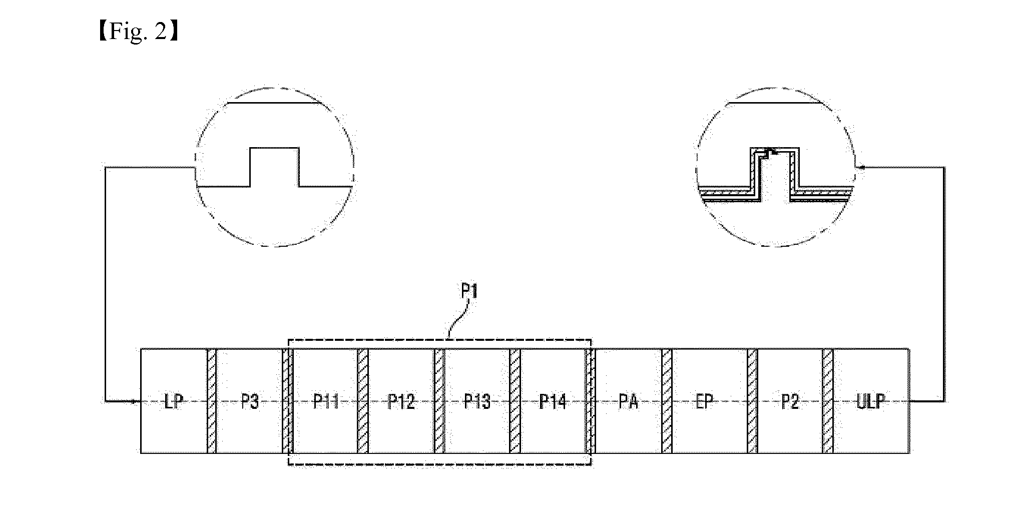
[0069]FIG. 3 shows an integrated thin film solar cell manufacturing apparatus with a double-junction structure according to a modified example of the present invention and shows an inline type manufacturing apparatus in a roll-to-roll method or in a roller method. Such an apparatus includes, as shown in FIG. 3, not only one or more unit process chambers P11 to P14 forming the first photoelectric converter but also one or more unit process chambers P11′ to P14′ forming the second photoelectric converter on the substrate where the first photoelectric converter has been formed. The plurality of unit process chambers P11′ to P14′ forming the second photoelectric converter may be connected between the unit process chamber P14 and the mask layer forming process chamber PA forming the mask layer.

[0070]As described with reference to the first embodiment, the integrated thin film solar cell manufacturing apparatuses according to the second embodiment and the modified example of the second em...

third embodiment

[0078]As described above, in the manufacture of the integrated solar cell by the inline type in a roll-to-roll method or in a roller method according to the present invention, it is possible to manufacture the integrated high efficiency thin film solar cell which has a multi junction structure and maximizes the effective area by performing repeatedly or continuously only a deposition process in the plurality of vacuum process chambers.

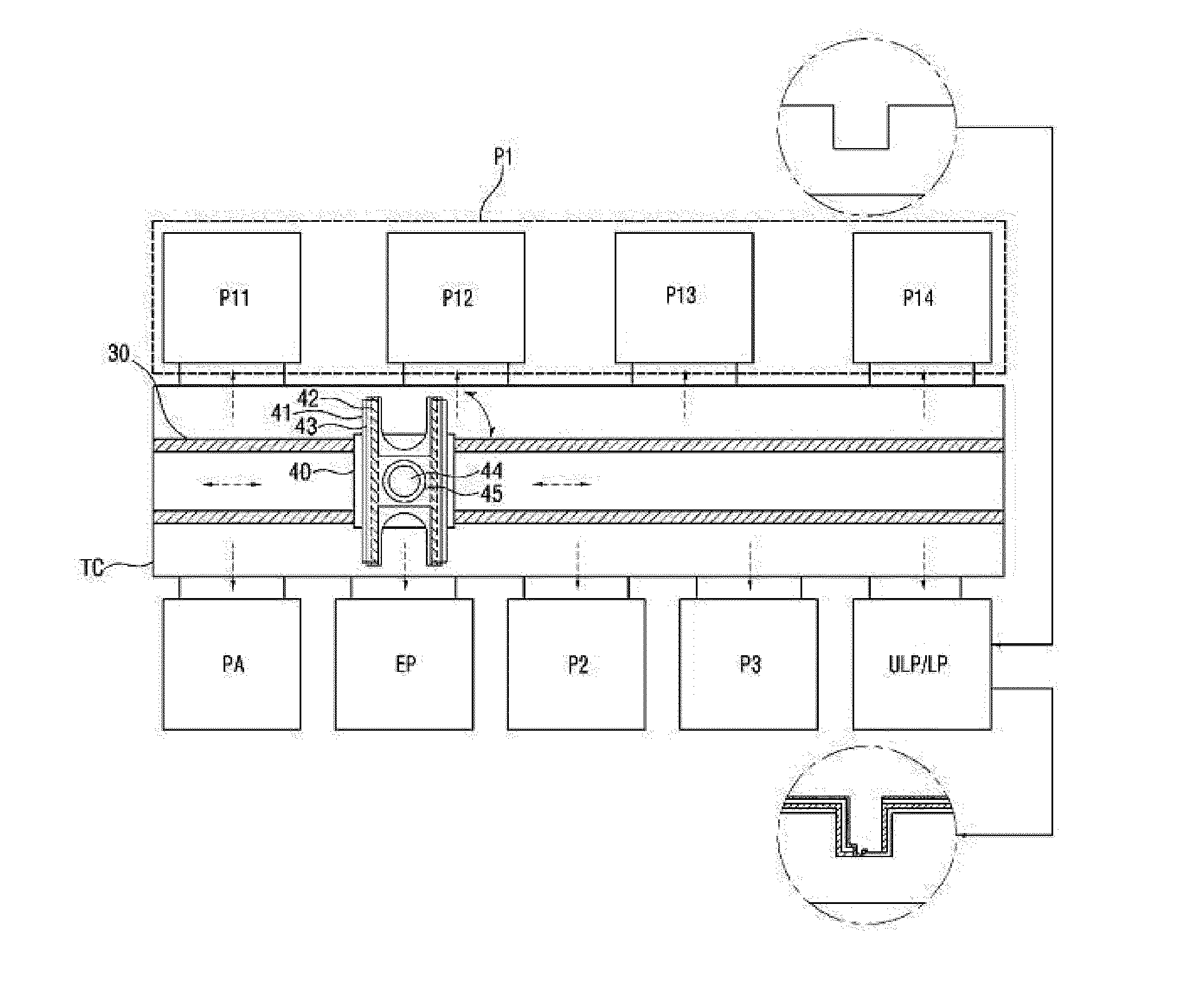
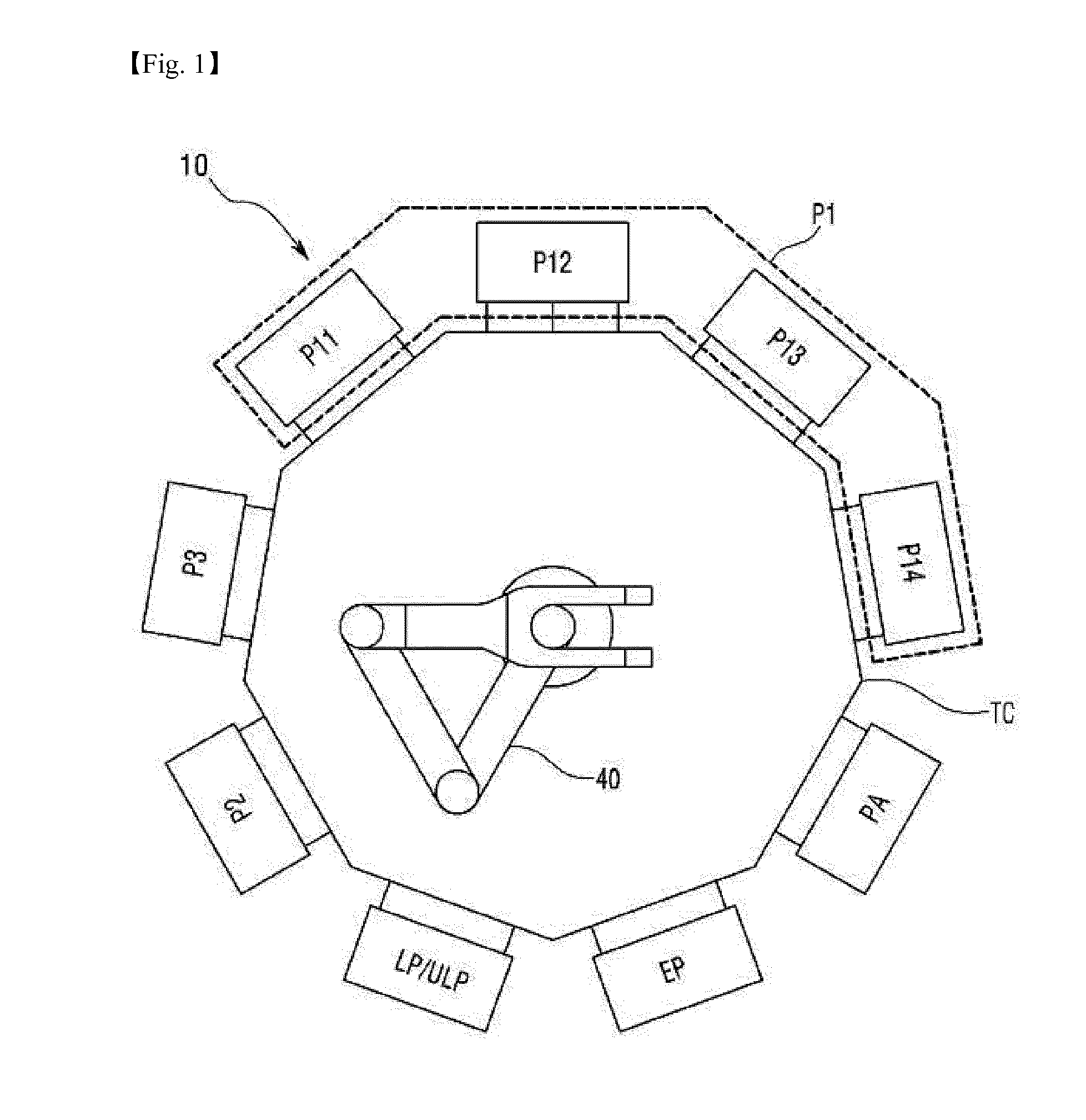
[0079]FIG. 4 shows an integrated thin film solar cell manufacturing apparatus according to a modified example of the first embodiment of the present invention and shows an inline type manufacturing apparatus in a cluster method.

[0080]Meanwhile, the integrated thin film solar cell manufacturing apparatus shown in FIG. 4 includes the photoelectric converter forming process chamber P1 including one or more unit process chambers P11, P12, P13, and P14, the mask layer forming process chamber PA, the etching process chamber EP, the second electrode layer for...


PUM


Abstract

An apparatus for manufacturing an integrated thin film solar cell in which a plurality of unit cells are electrically connected in series to each other in vacuum may be provided that includes: a photoelectric converter forming process chamber which forms a photoelectric converter by emitting a photoelectric conversion material on a substrate where a first conductive layer has been formed from one basic line within each of a plurality of trenches formed in the substrate to a bottom of each of the trenches, to one side continuous from the bottom, and to a protruding surface of the substrate, which is continuous from the one side; and a second conductive layer forming process chamber which forms a second conductive layer from another basic line within each of the trenches to the bottom of each of the trenches, to the other side continuous from the bottom, and to a protruding surface of the substrate, which is continuous from the other side. The photoelectric converter forming process chamber and the second conductive layer forming process chamber perform the respective processes in vacuum.

Description

TECHNICAL FIELD[0001]The present invention relates to apparatuses for manufacturing integrated thin film solar cells.BACKGROUND ART[0002]Generally, a solar cell is a device which converts sunlight energy into electric energy by using a photovoltaic effect caused by a junction of a p-type semiconductor and an n-type semiconductor, that is, a semiconductor p-n junction, by a junction of metal and semiconductor, that is, a metal / semiconductor (MS) junction (what is called, Schottky junction), or by a metal / insulator / semiconductor (MIS) junction.[0003]Based on a material used for the solar cell, the solar cell is largely divided into a silicon based solar cell, a compound based solar cell, and an organic based solar cell. According to a semiconductor phase, the silicon based solar cell is divided into a single crystalline silicon (sc-Si) solar cell, a polycrystalline silicon (pc-Si) solar cell, a microcrystalline silicon (μc-Si:H) solar cell, and an amorphous silicon (a-Si:H) solar cell...

Claims


Application Information

Patent Timeline
Patent Type & Authority Applications(United States)
IPC IPC(8): H01L31/0463H01L31/0465H01L31/18
CPCH01L31/0463H01L31/0465H01L31/18H01L31/046Y02E10/50H01L31/0445
Inventor LIM, KOENG SUJEON, JIN WANHONG, YUN HO
Owner KOREA ADVANCED INST OF SCI & TECH
Why Eureka
Try Eureka