Biometric recognition apparatus with deflection electrode

a biometric recognition and electrode technology, applied in the direction of acquiring/reconciling fingerprints/palmprints, pulse techniques, instruments, etc., can solve the problems of high material cost and package cost, huge noise,

Active Publication Date: 2016-11-24
SUPERC TOUCH CORP
View PDF6 Cites 9 Cited by
  • Summary
  • Abstract
  • Description
  • Claims
  • Application Information

AI Technical Summary

Benefits of technology

[0005]The conventional capacitive fingerprint sensors can be classified into swipe type and area type (pressing type), and the area type has better identification correctness, efficiency and convenience. However, the area type capacitive fingerprint sensor generally integrates the sensing electrodes and the sensing circuit into one integrated circuit (IC) protected by a sapphire film with thickness below 100 um because the sensed signals are minute and the background noise is huge in comparison with the minute sensed signals. As a result, the material cost and package cost is high and the product lifetime and durability are influenced. It is a development trend to enhance the sensing sensibility and signal-to-noise ratio for the sensing circuit such that the distance between the sensing electrode and user finger can be increased and the package of the sensing IC can be simplified. It is also desirable to integrate the sensing electrode to location below the protection glass or even more desirable to integrate the sensing electrode into the display panel, thus greatly reducing cost and enhancing product lifetime and durability.

Problems solved by technology

However, the area type capacitive fingerprint sensor generally integrates the sensing electrodes and the sensing circuit into one integrated circuit (IC) protected by a sapphire film with thickness below 100 um because the sensed signals are minute and the background noise is huge in comparison with the minute sensed signals.
As a result, the material cost and package cost is high and the product lifetime and durability are influenced.

Method used


Image

  • Biometric recognition apparatus with deflection electrode
  • Biometric recognition apparatus with deflection electrode
  • Biometric recognition apparatus with deflection electrode

Examples


Embodiment Construction

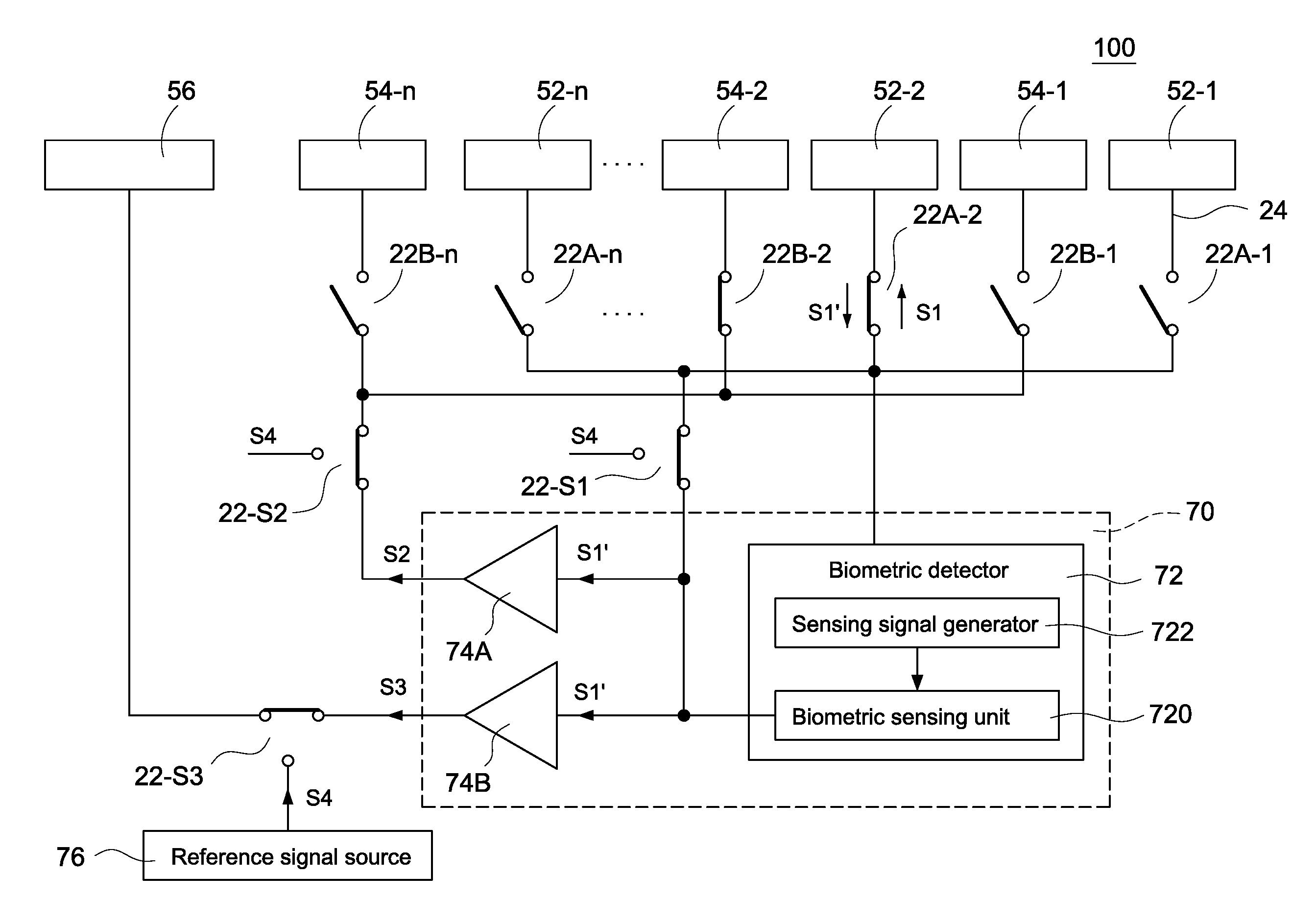
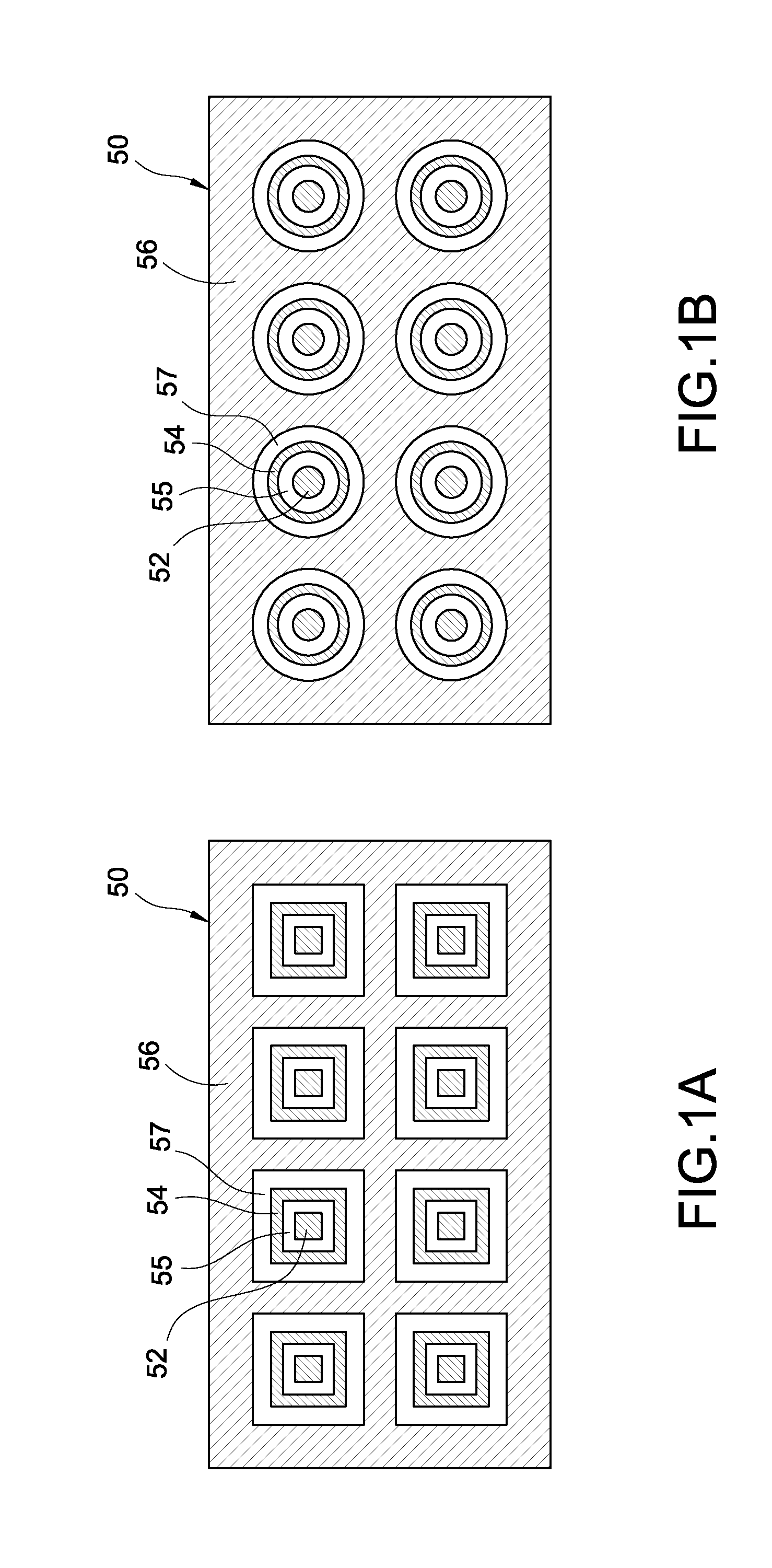
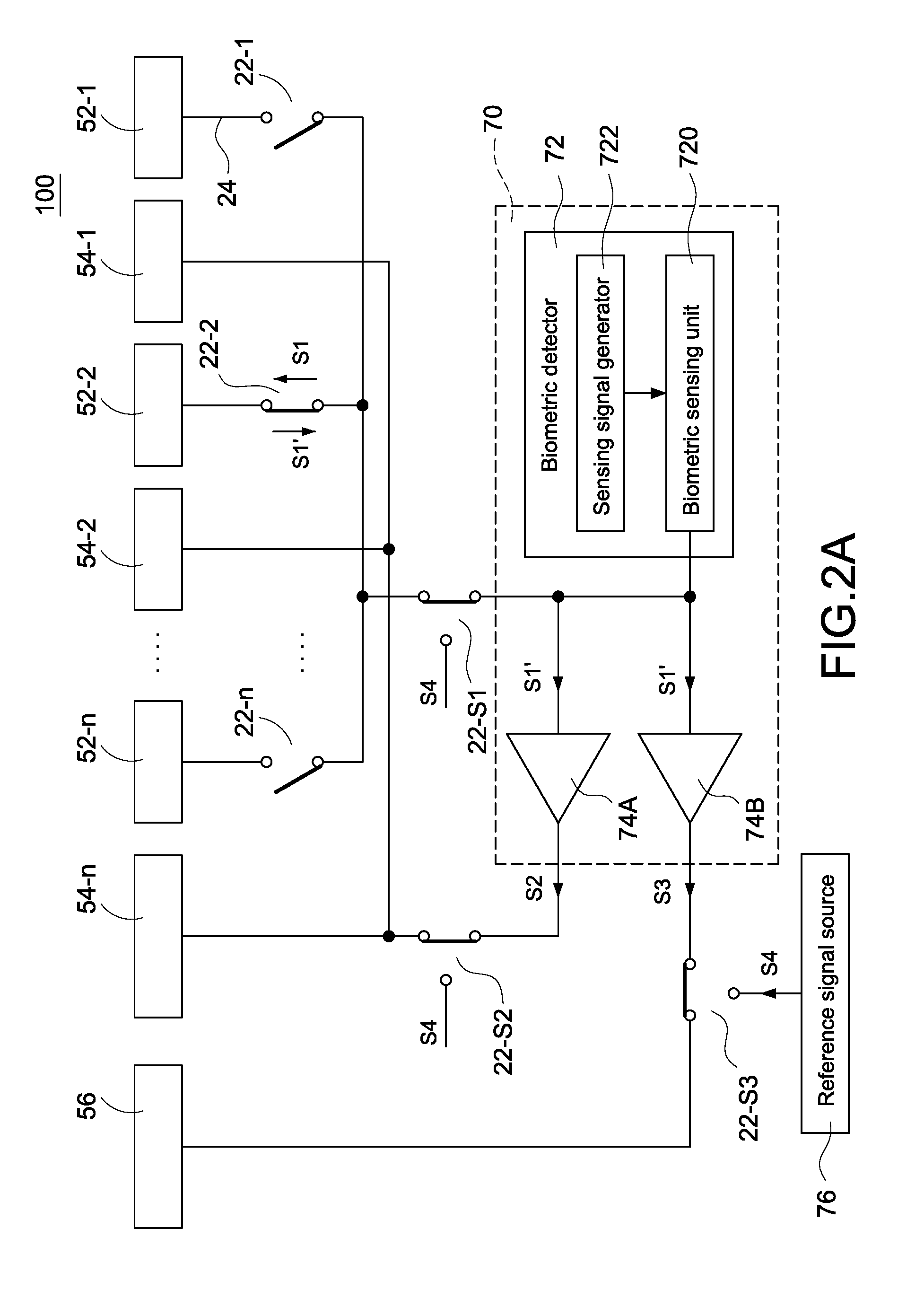
[0026]FIG. 1A is a top view showing the multi-function electrode layer 50 in the biometric recognition apparatus 100 according to an embodiment of the present invention. The multi-function electrode layer 50 comprises a plurality of sensing electrodes 52, a plurality of deflection electrodes 54 and at least one suppressing electrode 56. Each of the sensing electrodes 52 is at least partially surrounded by a corresponding deflection electrode 54. Each of the deflection electrodes 54 is at least partially surrounded by the suppressing electrode 56 such that the sensing sensibility and signal-to-noise ratio can be enhanced. The deflection electrode 54 at least partially surrounds one corresponding sensing electrode 52 and electrically isolated with the surrounded sensing electrode 52. For example, the deflection electrode 54 may completely surround one corresponding sensing electrode 52 as shown in FIG. 1A. According to one embodiment, the sensing electrode 52 may be of rectangular sha...


PUM


Abstract

A biometric recognition apparatus with deflection electrode includes a substrate, a multi-function electrode layer including a plurality of sensing electrodes, a plurality of deflection electrodes and at least one suppressing electrode. Each of the sensing electrodes is at least partially surrounded by a corresponding deflection electrode and each of the deflection electrodes is at least partially surrounded by the suppressing electrode. The biometric recognition apparatus further includes a switching circuit layer having a plurality of selection switches and conductive wires, at least a part of the selection switches and the conductive wires are electrically connected to the sensing electrodes. By above arrangement of the sensing electrodes, the deflection electrodes and the suppressing electrode, the sensing sensibility and signal to noise ratio can be enhanced, thus increasing the sensing distance between sensing electrode and user finger.

Description

BACKGROUND OF THE INVENTION[0001]1. Field of the Invention[0002]The present invention relates to a biometric recognition apparatus, especially to a biometric recognition apparatus with deflection electrode.[0003]2. Description of Prior Art[0004]Biometric recognition technology has been widely applied to personal identification and authentication. The conventional biometric recognition technologies can be classified into fingerprint recognition, iris recognition or DNA recognition and so on. Due to safety, non-invasiveness and efficiency considerations, fingerprint recognition becomes main stream technology. The fingerprint recognition device can scan fingerprint image by optical scanning, thermal imaging, supersonic imaging or capacitive imaging. For compactness, cost, power-saving, reliability and security concerns, the capacitive fingerprint sensor becomes popular for biometric recognition technology applied to portable electronic devices.[0005]The conventional capacitive fingerpr...

Claims


Application Information

Patent Timeline
Patent Type & Authority Applications(United States)
IPC IPC(8): G06K9/00H03K17/96H05K1/02
CPCG06K9/0002H05K1/0274H03K2217/960765H03K17/9622H05K1/0296G06V40/1306H03K2217/96023H05K1/162H05K2201/10151
Inventor LEE, HSIANG-YUCHIN, SHANGLIN, PING-TSUN
Owner SUPERC TOUCH CORP
Why Eureka
Try Eureka