

Methods for in-plane strain measurement of a substrate
- Summary
- Abstract
- Description
- Claims
- Application Information
AI Technical Summary
Benefits of technology
Problems solved by technology
Method used
Image

Examples
example 1
Demonstration of Strain Sensing Using Laser Scanning Technique: Strain Sensitivity and Spatial Resolution
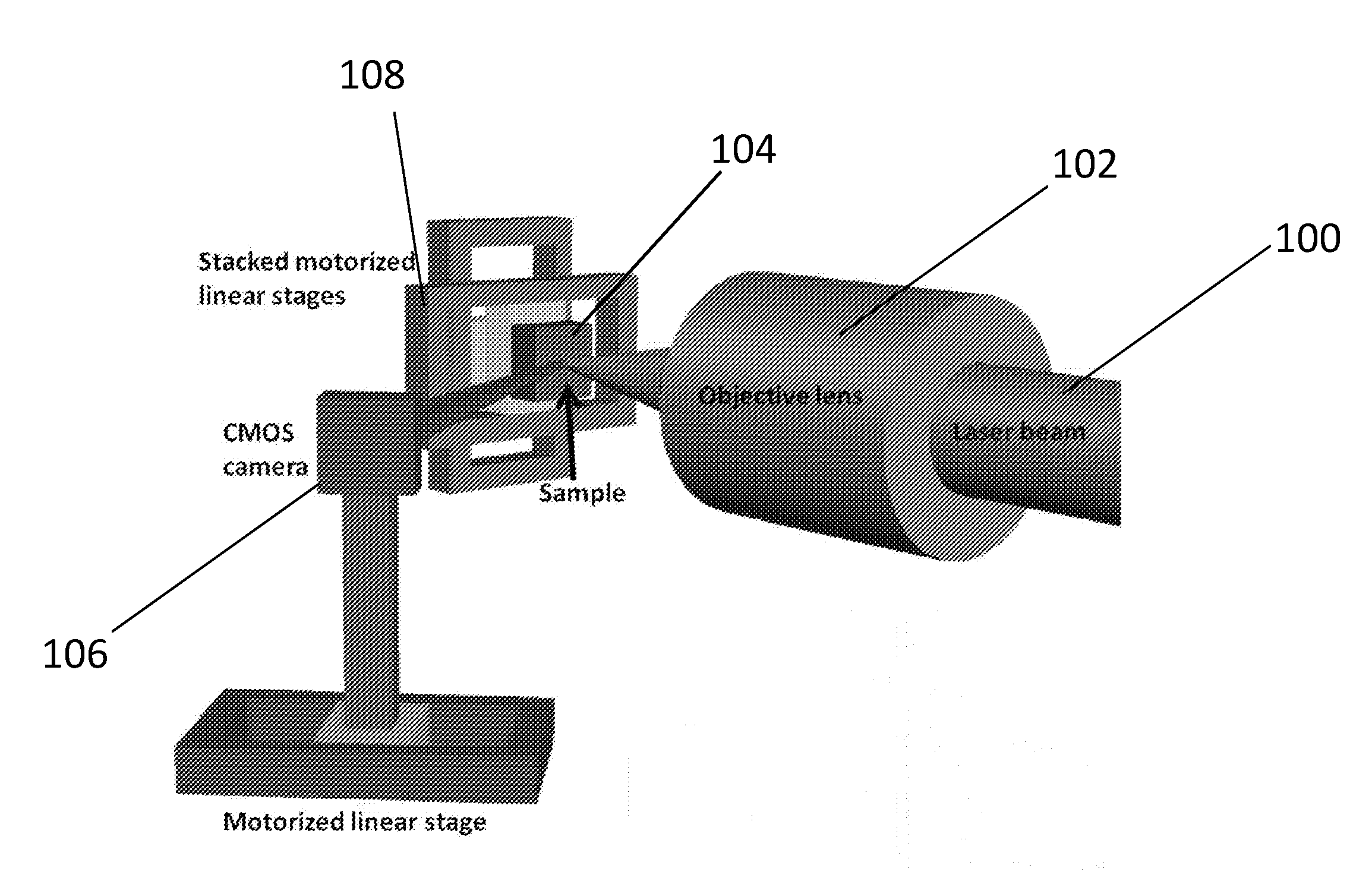
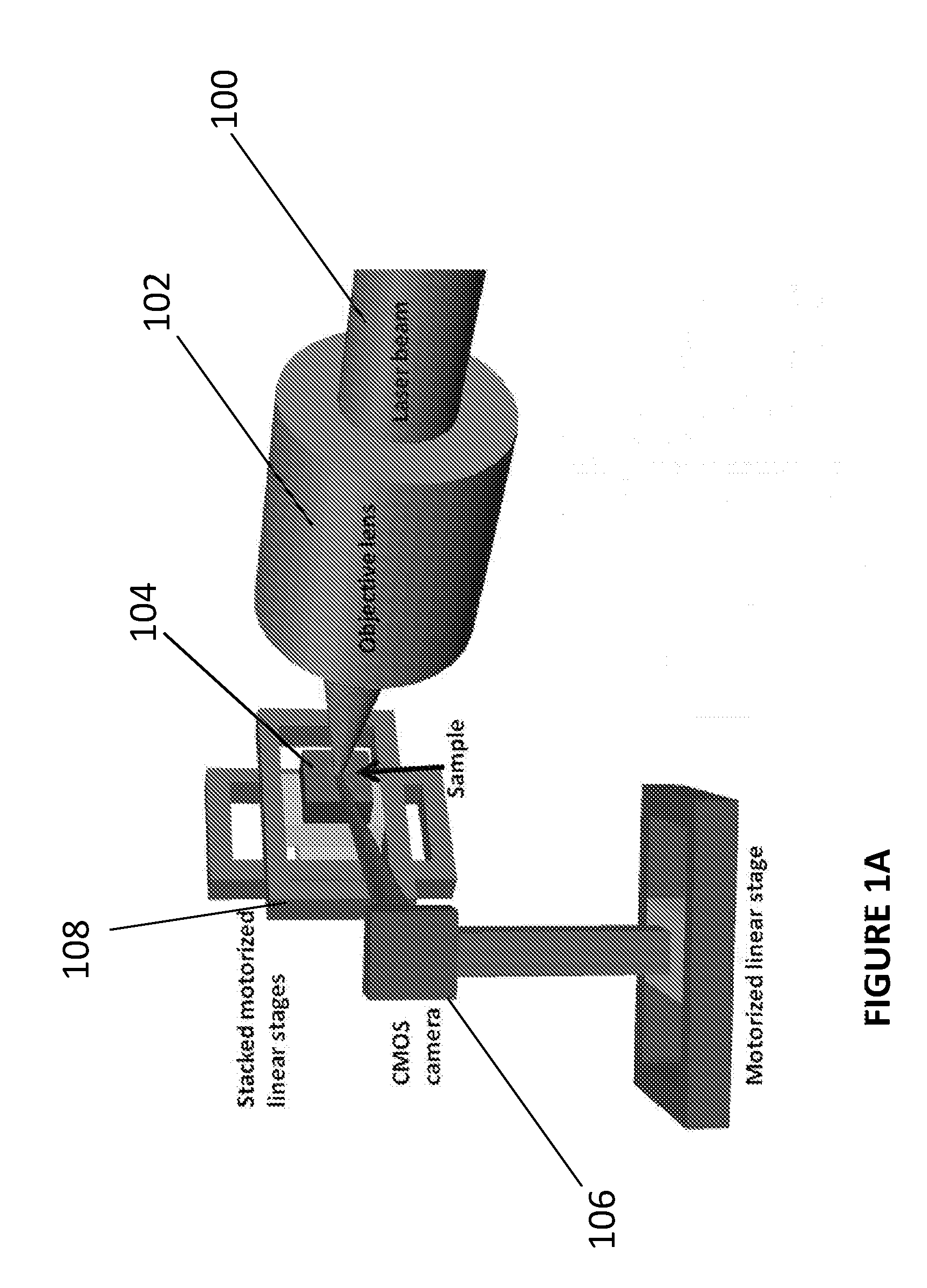
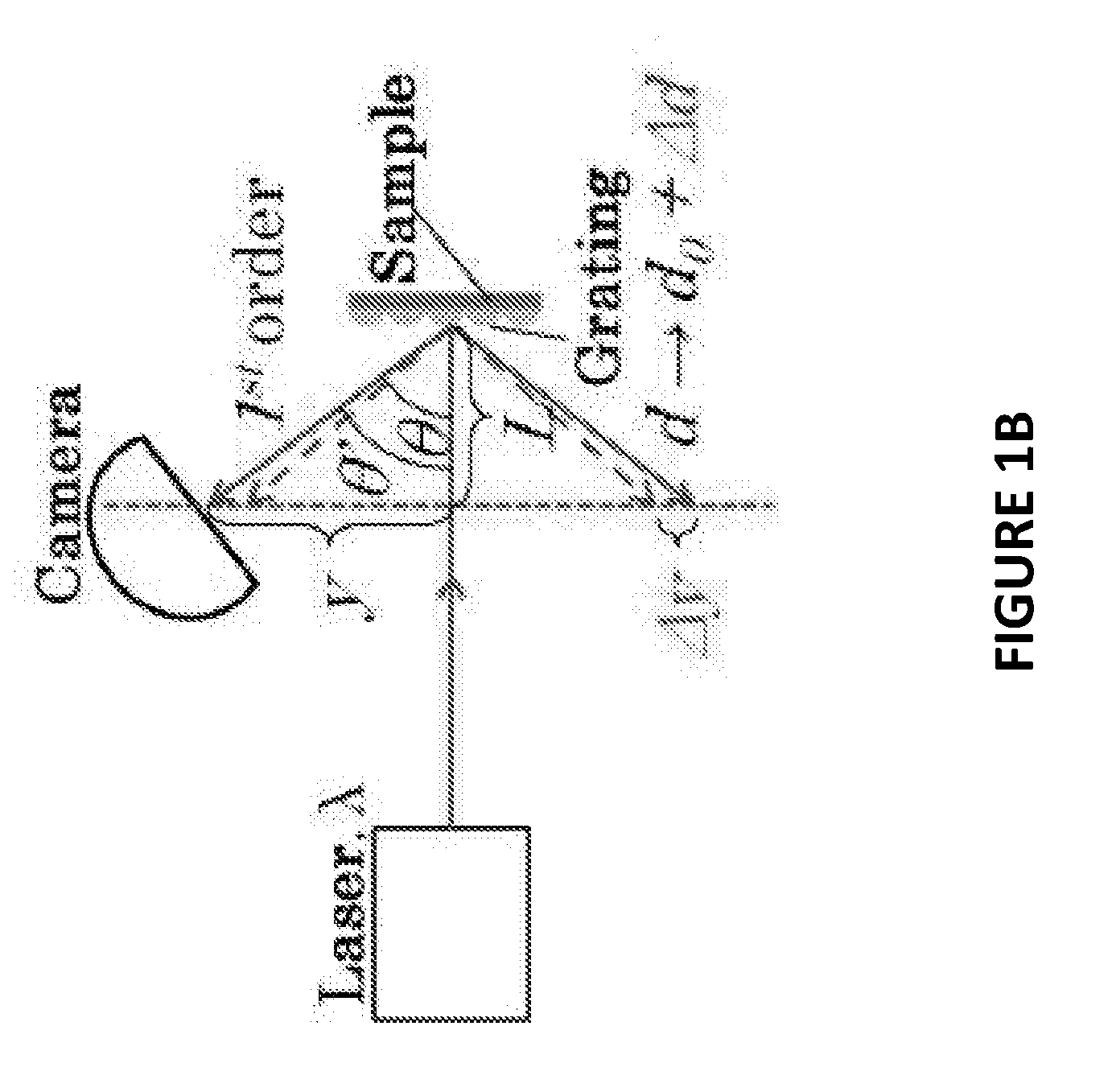
[0058]The spatial resolution is studied using a specially designed grating pattern on a polished silicon substrate made with electron beam lithography (EBL) in this work. Alternatively, for a large area, sub-micron periodic grating structure, soft material contact lithography can be used. The grating wavelength is spatially varied on the substrate to model the strain distribution, where the strain is defined as Δd / d0. By scanning the laser beam across the whole grating pattern, one can obtain the grating wavelength d versus the laser spot's position on the sample. By comparing the extracted grating wavelength distribution from the experiment with the original design, one can study the spatial resolution and accuracy of the strain sensing. The strain sensitivity is validated by extracting the coefficient of thermal expansion from silicon.
[0059]The EBL defined pattern, shown in FIG...
example 2
Fabrication and Finite Element Analysis (FEA) of a Planarized Junction of SU-8 / Si
[0064]In order to obtain the strain information at the junction of two dissimilar materials with different CTEs upon thermal loading, we fabricated a globally planarized junction composed of SU-8 / Si. The fabrication of the SU-8 / Si starts from a silicon on insulator (SOI) wafer. The top silicon layer is 10-20 μm thick and is patterned into silicon strips using a standard lithography process. The width of the silicon strips and the spacing are in the range of tens of microns to several hundreds of microns. Then an SU-8 layer is spin-coated on top to fill in the trenches completely. After hard-baking the SU-8 layer, deep reactive ion etching (DRIE) is used to etch the silicon substrate from the backside until the SiO2 etch stop layer, which is then removed at the subsequent step using hydrofluoric acid (HF). FIG. 7A shows the scanning electron microscopy (SEM) image of a SU-8 / Si junction, and FIG. 7B shows...
example 3
Strain Mapping On SU-8 / Si Composite Sample
[0068]Electronic packages are typically integrated with various different materials with a mismatched CTE, which leads to a complicated distribution of strain across the whole package. To evaluate the applicability of this laser scanning technique for strain mapping, we tested a composite sample as described in the preceding section to model a simplified case of strain distribution. The results were compared with thermal strain distributions calculated by FEA for a similar sample structure. The comparison between the measurement and simulation results evaluates the feasibility of applying this laser scanning technique towards advanced applications of electronic packages.
[0069]We first fabricated a uniform grating structure with an 800 nm wavelength across consecutive SU-8 / Si strip samples using EBL and metal lift-off techniques. Ideally, for a uniform material, the grating wavelength will not change across the sample. After heating the compo...
PUM
 Abstract
Description
Claims
Application Information