
Integrated target waveguide devices and systems for optical coupling

Active Publication Date: 2016-12-15
PACIFIC BIOSCIENCES
View PDF9 Cites 63 Cited by
  • Summary
  • Abstract
  • Description
  • Claims
  • Application Information

AI Technical Summary

Benefits of technology

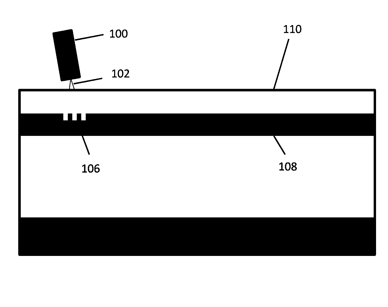
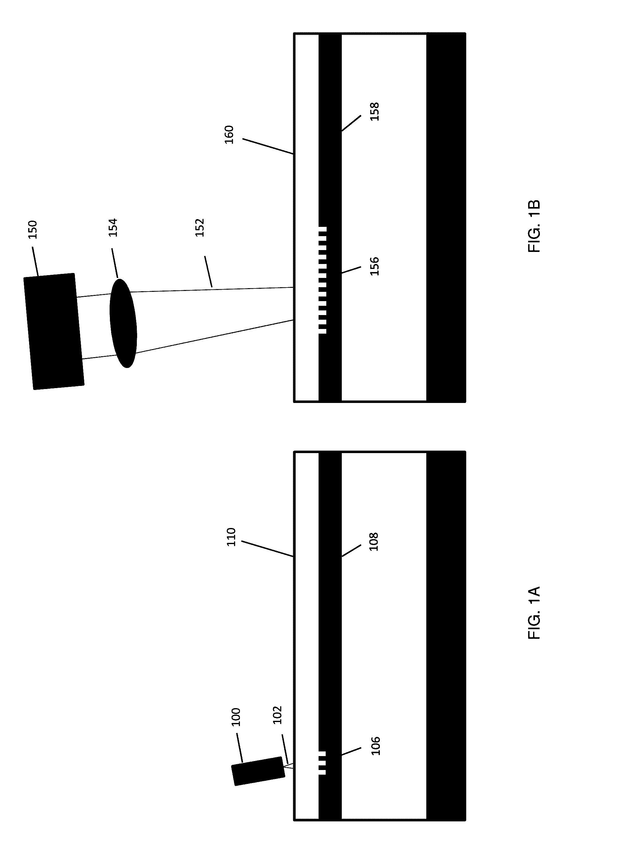
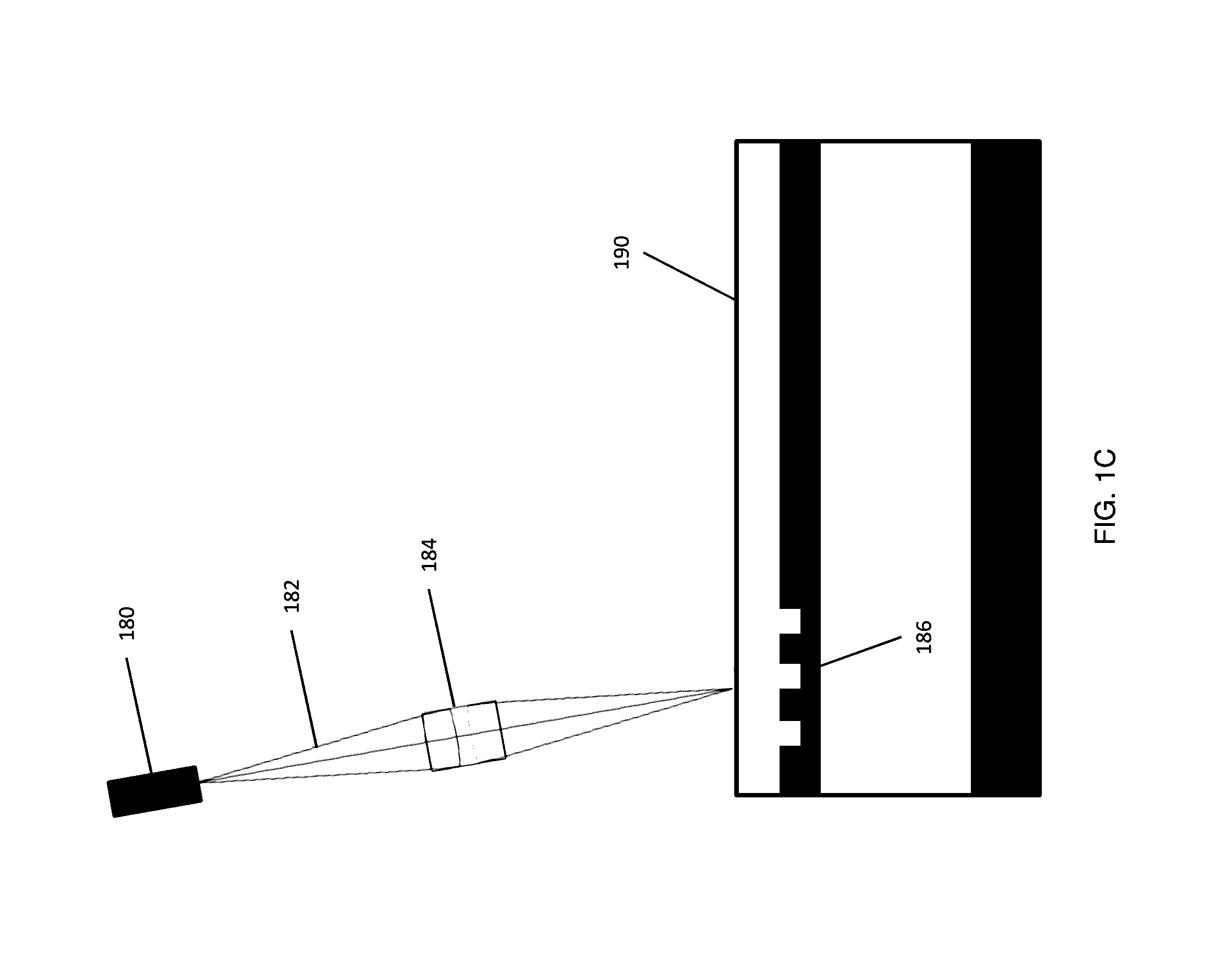
The present disclosure provides an integrated target waveguide device comprising a low numerical aperture coupler and an integrated waveguide optically coupled to the coupler. The device is at least 100 μm2 in size. The coupler is designed to minimize signal loss and facilitate optical coupling with external optical sources. The disclosed device can be used in various optical analytical systems. The technical effects of the invention include improved optical coupling, reduced signal loss, and improved optical analysis.

Problems solved by technology

Such systems are frequently complex and costly and tend to have significant space requirements.
Such close and irreversible associations between an optical source and its target device are thus not well suited for use in analytical systems having a removable sample holder, where the optical output from an optical source, such as a traditional optical train, is normally coupled to the target sample holder through free space.
In addition, the integrated optical circuits typically used in telecommunications applications are not designed to carry the intensity of optical energy necessary to analyze the large numbers of nanoscale samples present in the highly-multiplexed analytical systems described above, nor are they designed for use with optical sources having wavelengths suitable for use in optical systems with standard biological reagents.
For example, where a target device comprises an integrated optical waveguide for routing the optical energy through the device, launching of the optical energy into the waveguide can be unreliable and inefficient.
Depending on the implementation, however, each approach has limitations with respect to efficiency, reliability, applicability, cost, and the like.

Method used


Image

  • Integrated target waveguide devices and systems for optical coupling
  • Integrated target waveguide devices and systems for optical coupling
  • Integrated target waveguide devices and systems for optical coupling

Examples


example 1

Binary Grating Couplers with Low Numerical Aperture

[0205]This example describes the design, optimization, and modeling of various binary grating couplers having low NA. The coupling of optical energy through free space to a 2-dimensional grating coupler can be modeled using finite-difference time-domain (FDTD) numerical analysis of the Maxwell equations, for example using computer software from Lumerical (www.lumerical.com) or the like. An example of such modeling is shown in FIG. 17A, where the 2-dimensional Gaussian light source (1702) is shown in light shading above the device model. The arrow shown within the light source represents a coupling angle of 10 degrees. The arrow is shown intersecting a rectangular box that represents the grating coupler structure (1704). The oxide cladding (1706) is the solid layer surrounding the coupler. The waveguide core (1708) is represented as a thin line extending to the left from the coupler. Optical energy is coupled from above the structure...

example 2

Estimation of Coupling Efficiencies into Model Target Waveguide Device

[0212]This example provides estimated coupling efficiencies for a waveguide device with an Si3N4 core with dimensions roughly 0.600×0.050 μm, surrounded by SiO2 cladding, and supporting a single TM0 mode.

Coupling efficiency:

ηtargetdevice=PoweringuidedmodeTotalpowerindevice

Waveguide effective index:

ne=βk=1.9

λ=532 nm, k=1.18×10⁻⁹ cm−1

β=1.87×105 cm−1

κ=coupling coefficient (mode overlap integral)

Maximum condition: ηL=π / 2

Requirement for minimum radius of curvature: 0.9 mm

Radiative loss per bend: 0.5 dB

[0213]A not-to-scale representation of the exemplary waveguide cross-section is shown in FIG. 23A. Estimates of coupling efficiency are based on a calculation of the overlap integral between the desired mode profile and the excitation field. An analytics solution of the fields for this geometry is not known, but the basic mode profile of the TE0 mode of this waveguide can be approximated (Schlosser and Unger, based on a...

example 3

Theoretical Transverse Coupling into Waveguide Device with a Polished Facet

[0214]The overall coupling efficiency of a device with a polished facet is the product of reflectance loss and mode overlap, where reflection loss for free-space coupling is larger than for an incident plane wave: 9.6%. Perfect coupling would require an incident energy distribution that is exactly the inverse of the far-field distribution of light exiting the guide. A more accurate calculation of the reflectance loss, however, would require integration over these angles. The result of integrating over the high NA dimension only is 12.4%. The best-case insertion loss of the device under a straightforward approach is

ηinstrument=0.876

The efficiency could be improved by applying an AR coating. The efficiency could also be improved by including a very small air gap—on the order of the light wavelength—between the target device and the exit facet of the illumination source.

[0215]Efficiencies are determined by the m...


PUM


Abstract

Integrated target waveguide devices and optical analytical systems comprising such devices are provided. The target devices include an optical coupler that is optically coupled to an integrated waveguide and that is configured to receive optical input from an optical source through free space, particularly through a low numerical aperture interface. The devices and systems are useful in the analysis of highly multiplexed optical reactions in large numbers at high densities, including biochemical reactions, such as nucleic acid sequencing reactions. The devices provide for the efficient and reliable coupling of optical excitation energy from an optical source to the optical reactions. Optical signals emitted from the reactions can thus be measured with high sensitivity and discrimination. The devices and systems are well suited for miniaturization and high throughput.

Description

CROSS-REFERENCE TO RELATED APPLICATIONS[0001]This application claims the benefit of U.S. Provisional Application No. 62 / 175,139, filed on Jun. 12, 2015, the disclosure of which is incorporated herein by reference in its entirety.BACKGROUND OF THE INVENTION[0002]As multiplexed optical analytical systems continue to be miniaturized in size, expanded in scale, and increased in power, the need to develop improved systems capable of delivering optical energy to such systems becomes more important. For example, highly multiplexed analytical systems comprising integrated waveguides for the illumination of nanoscale samples are described in U.S. Patent Application Publication Nos. 2008 / 0128627 and 2012 / 0085894. Further optical systems for the analysis of nanoscale samples, including the illumination and detection of such samples, are described in U.S. Patent Application Publication Nos. 2012 / 0014837, 2012 / 0021525, and 2012 / 0019828. Additional nanoscale illumination systems for highly multip...

Claims


Application Information

Patent Timeline
IPC IPC(8): G02B6/124G01N21/77G01N21/64G02B6/42G01N21/03
CPCG02B6/124G02B6/4221G01N21/03G01N2021/0346G01N21/774G02B2006/12135G01N21/6486G02B6/34G01N21/6452G01N21/648G01N21/7703
Inventor WANG, SHANGFOQUET, MATHIEULUNDQUIST, PAULRULISON, AARONMCDONALD, MARKHERRMANN, ARIEL
Owner PACIFIC BIOSCIENCES
Learn More