GaN SEMICONDUCTOR DEVICE STRUCTURE AND METHOD OF FABRICATION BY SUBSTRATE REPLACEMENT

a technology of gan transistor and substrate, which is applied in the direction of semiconductor/solid-state device testing/measurement, semiconductor device details, semiconductor/solid-state device testing/measurement, etc., can solve the problems of poor thermal dissipation of sic substrate relative to sic substrate, significant influence of breakdown voltage and thermal dissipation of gan transistor, and the limitation of maximum breakdown voltage of silicon substra

Active Publication Date: 2016-12-29
GAN SYST
View PDF5 Cites 52 Cited by
  • Summary
  • Abstract
  • Description
  • Claims
  • Application Information

AI Technical Summary

Benefits of technology

[0066]Thus, there is provided a nitride semiconductor device structure and a method of fabrication thereof, for increased vertical breakdown resistance and improved thermal dissipation relative to GaN-on-Si device structures. In particular, the device structure and method of fabrication is applicable for GaN devices and systems comprising one or more lateral GaN power transistors.

Problems solved by technology

The substrate material on which a GaN transistor is fabricated can significantly affect the breakdown voltage and thermal dissipation.
However, a known issue with GaN-on-Si devices, e.g. a GaN HEMT fabricated as a GaN / AlGaN epi-layer stack on a silicon substrate, is that the maximum breakdown voltage is limited by the silicon substrate, and is typically less than 400V.
Another drawback is poorer thermal dissipation of Si substrates relative to SiC substrates.
However, sapphire substrates have other drawbacks relative to silicon substrates, including, high cost, limited available wafer size and poor thermal conductivity.
However, these substrates have poorer thermal conductivity than silicon or silicon carbide.
While they improve breakdown voltage, lack of thermal dissipation leads to high operational temperatures, which adversely affects device performance, and / or causes early device failure.
However, as taught by Chao(5), bonding of a GaN epi-layer structure to a diamond substrate requires specialized processing, and there is a significant mismatch of the Coefficient of Thermal Expansion (CTE) between GaN and diamond.
Alternative growth substrates, and alternative substrates for epitaxial transfer, such as diamond or sapphire, are currently available only as smaller diameter wafers, and require more costly processing and wafer bonding.
These substrates result in significantly higher fabrication costs per unit area compared to silicon substrates.

Method used


Image

  • GaN SEMICONDUCTOR DEVICE STRUCTURE AND METHOD OF FABRICATION BY SUBSTRATE REPLACEMENT
  • GaN SEMICONDUCTOR DEVICE STRUCTURE AND METHOD OF FABRICATION BY SUBSTRATE REPLACEMENT
  • GaN SEMICONDUCTOR DEVICE STRUCTURE AND METHOD OF FABRICATION BY SUBSTRATE REPLACEMENT

Examples


Embodiment Construction

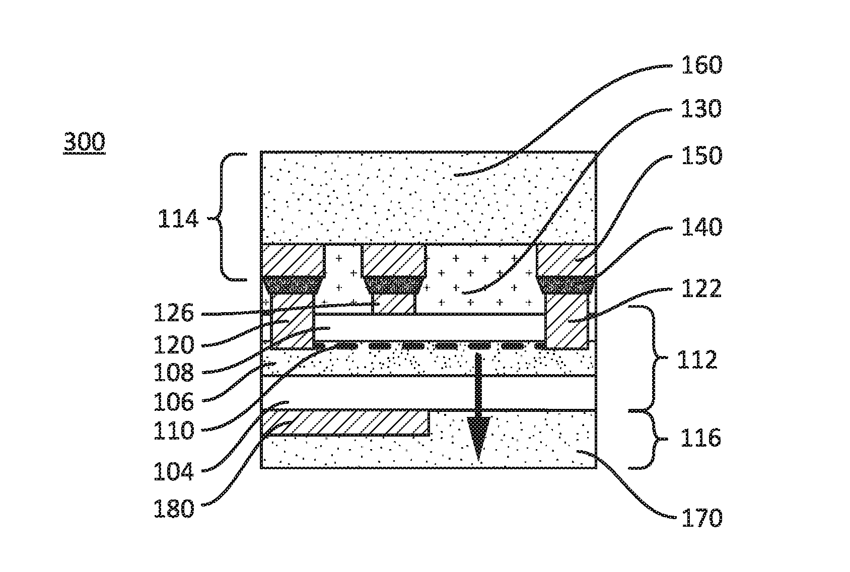
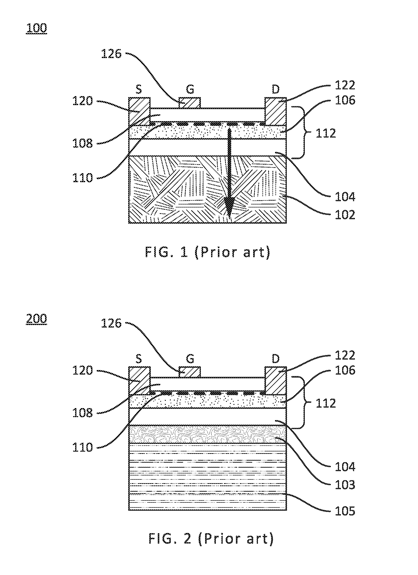
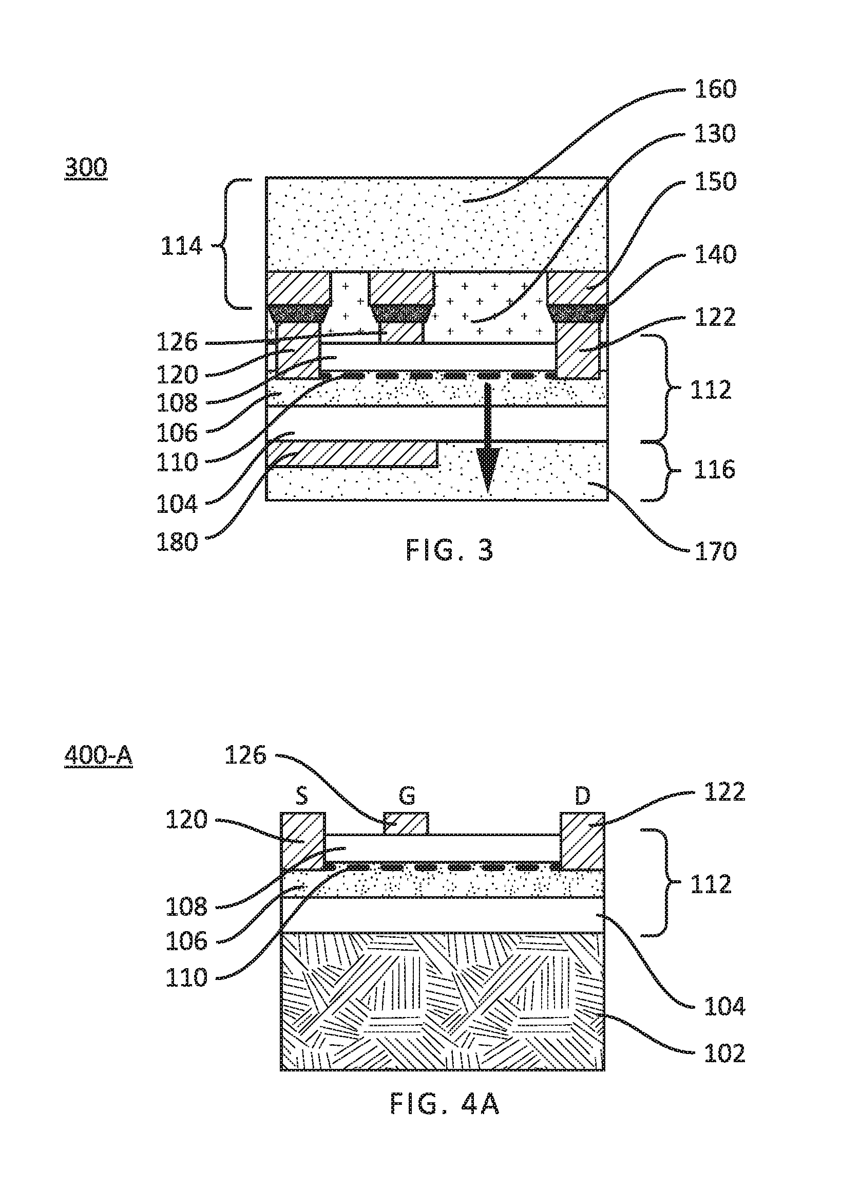
[0077]FIG. 1 illustrates schematically a simplified cross-sectional view of a conventional device structure 100, comprising a lateral GaN power transistor, fabricated on a silicon substrate 102. The GaN semiconductor layers comprise one or more buffer layers or intermediate layers 104, a GaN layer 106, and an overlying AlGaN layer 108, which are formed epitaxially on the native silicon substrate 102. The latter may be referred to as the growth substrate. The GaN / AlGaN heterostructure layers 106 / 108 create a 2DEG active region 110 in device regions of the GaN-on-Si substrate. The stack of GaN epitaxial layers that is formed on the silicon substrate, i.e. intermediate layers 104, GaN layer 106, and AlGaN layer 108, and any intervening layers not actually illustrated, will be referred to below as the “epi-layer stack” or “epi-stack”112. After formation of the epi-stack 112, source, drain and gate electrodes are formed. For example, a conductive metal layer, e.g. a layer of aluminum / tit...


PUM


Abstract

Devices and systems comprising high current/high voltage GaN semiconductor devices are disclosed. A GaN die, comprising a lateral GaN transistor, is sandwiched between an overlying header and an underlying composite thermal dielectric layer. Fabrication comprises providing a conventional GaN device structure fabricated on a low cost silicon substrate (GaN-on-Si die), mechanically and electrically attaching source, drain and gate contact pads of the GaN-on-Si die to corresponding contact areas of conductive tracks of the header, then entirely removing the silicon substrate. The exposed substrate-surface of the epi-layer stack is coated with the composite dielectric thermal layer. Preferably, the header comprises a ceramic dielectric support layer having a CTE matched to the GaN epi-layer stack. The thermal dielectric layer comprises a high dielectric strength thermoplastic polymer and a dielectric filler having a high thermal conductivity. This structure offers improved electrical breakdown resistance and effective thermal dissipation compared to conventional GaN-on-Si device structures.

Description

CROSS-REFERENCE TO RELATED APPLICATION(S)[0001]This application is related to United States provisional patent application No. 62 / 260,275, filed Nov. 26, 2015, entitled “GaN SEMICONDUCTOR DEVICE STRUCTURE AND METHOD OF FABRICATING BY SUBSTRATE REPLACEMENT”; U.S. provisional patent application No. 62 / 209,930, filed Aug. 26, 2015, entitled “GaN SEMICONDUCTOR DEVICE STRUCTURE AND METHOD OF FABRICATION BY SUBSTRATE REPLACEMENT FOR INCREASED VERTICAL BREAKDOWN RESISTANCE OF GaN POWER TRANSISTORS”; and U.S. provisional patent application No. 62 / 185,124, filed Jun. 26, 2015, entitled “SUBSTRATE REPLACEMENT FOR INCREASED VERTICAL BREAKDOWN RESISTANCE OF GaN POWER TRANSISTORS”, all of which are incorporated herein by reference in their entirety.[0002]This application is related to PCT International Patent Application No. PCT / CA2014 / 00762, filed Oct. 28, 2014 and U.S. patent application Ser. No. 14 / 568,507, filed Dec. 12, 2014, both entitled “FAULT TOLERANT DESIGN FOR LARGE AREA NITRIDE SEMIC...

Claims


Application Information

Patent Timeline
Patent Type & Authority Applications(United States)
IPC IPC(8): H01L29/778H01L29/205H01L21/66H01L23/528H01L29/06H01L29/40H01L23/34H01L29/20H01L27/095
CPCH01L29/7787H01L29/2003H01L29/205H01L22/32H01L23/528H01L29/0669H01L29/402H01L23/34H01L27/095H01L29/7786H01L29/0619H01L23/36H01L23/3737H01L2224/81H01L22/14
Inventor ROBERTS, JOHNKLOWAK, GREG P.MCKNIGHT-MACNEIL, CAMERON
Owner GAN SYST
Why Eureka
Try Eureka