
Boron-doped n-type silicon target

a boron-doped n-type silicon and target technology, applied in the field of sputtering targets, can solve the problems of short target life and decreasing target life of p-type silicon

Inactive Publication Date: 2017-01-26
TOSOH SMD
View PDF2 Cites 2 Cited by
  • Summary
  • Abstract
  • Description
  • Claims
  • Application Information

AI Technical Summary

Benefits of technology

The patent text describes a new type of silicon sputter target that has specific electrical properties and contains a small amount of boron. The targets are made by measuring the resistivity of a single crystal silicon ingot, and then creating blanks from that ingot that meet the desired electrical properties. These blanks are then shaped into targets. The method does not involve any heat treatment after the ingot is prepared. The resistivity of the targets ranges from 0.1 to 700 ohm-cm, with 0.1-7 ohm-cm being the most common range. Using these targets in sputtering can improve the efficiency and performance of the sputtering process.

Problems solved by technology

Target life using p-type silicon is short.
This redeposition creates p-n junctions on the target surface, which under bias results in the presence of stress in the target, leading to target cracking, thus decreasing target life.

Method used


Image

  • Boron-doped n-type silicon target
  • Boron-doped n-type silicon target
  • Boron-doped n-type silicon target

Examples


Embodiment Construction

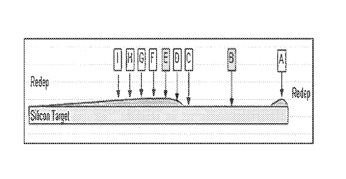
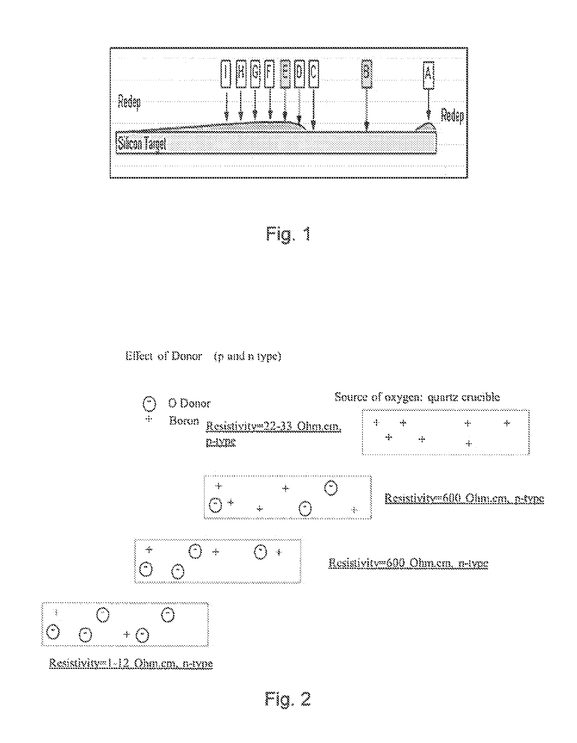
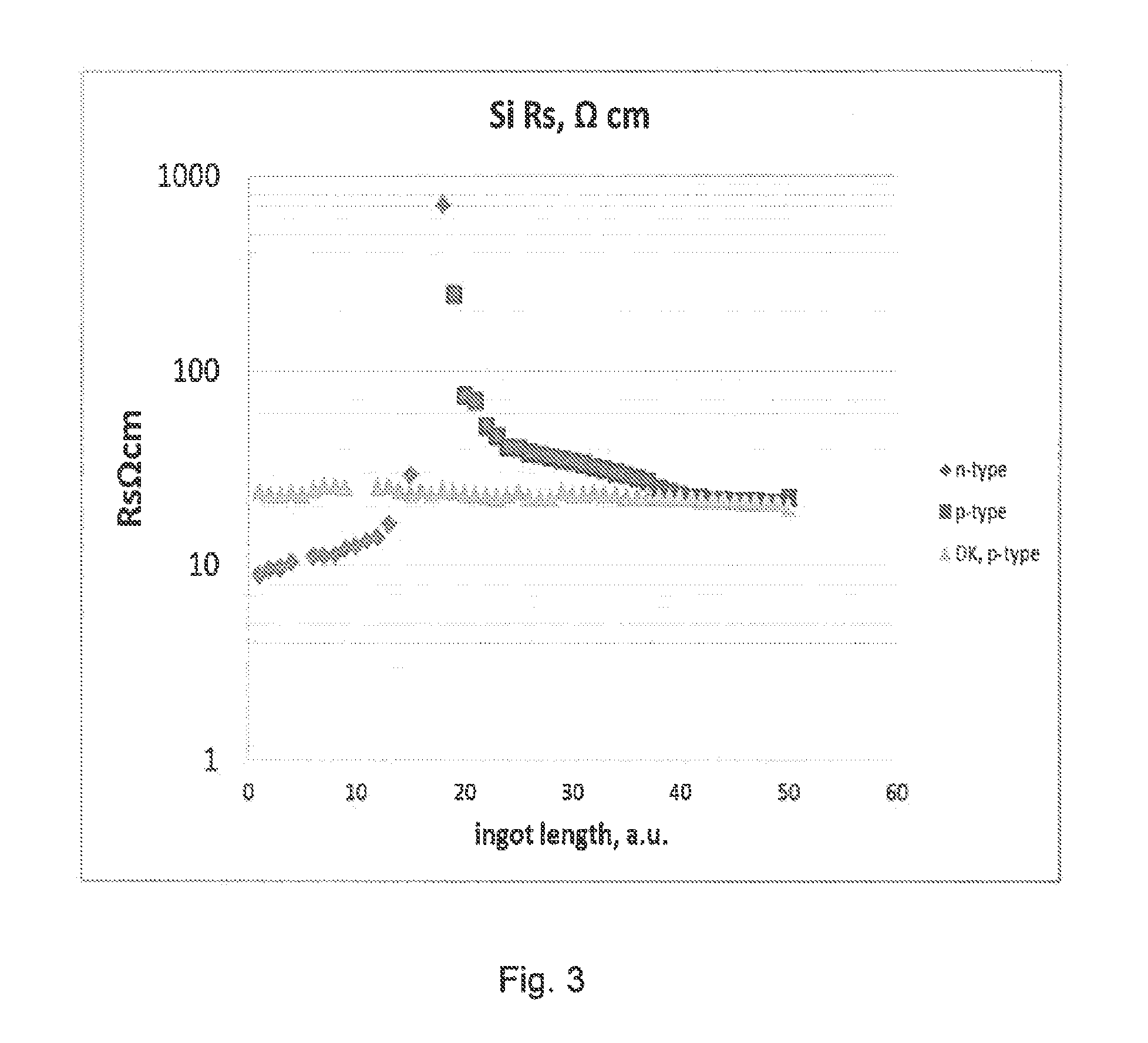
[0013]During growing of a high resistivity Czochralski (CZ) silicon ingots (1-100 ohm.cm range), there is certain amount of interstitial oxygen incorporated and formed oxygen thermal donors in silicon ingot material during crystal growth from silica crucible. The formation of oxygen thermal donors depends strongly on both interstitial oxygen concentration which is determined by process temperature and equilibrium between solid silica, liquid silicon, and solid silicon. To provide a certain silicon single crystal resistivity (1-100 ohm.cm), a certain amount of boron dopant is added to silicon. This added boron provides p-type carriers and determines p-type nature of silicon conductivity. The oxygen thermal donors contribute electrons to conduction. Depending on the number of donors generated and the amount of p-type carriers, the background carrier (boron) silicon may be of n-type (more n-type carriers) or p-type (more p-type carriers). In p-type silicon, oxygen thermal donors increa...


PUM

PropertyMeasurementUnit
Temperatureaaaaaaaaaa
Fractionaaaaaaaaaa
Fractionaaaaaaaaaa

Abstract

Sputter targets and methods of making same. The targets comprise B doped n-type Si. The targets may be made from single crystal boron doped p-type Si ingot made by the CZ method. Resistivities along the length of the crystal are measured, and blanks may be cut perpendicular to the ingot central axis at locations having resistivities of from about 1-20 ohm.cm. The blanks are then formed to acceptable shapes suitable for usage as sputter targets in PVD systems. No donor killing annealing is performed on the ingot or blanks.

Description

CROSS-REFERENCE TO RELATE APPLICATION[0001]This application claims the priority benefit of U.S. Provisional Patent Application Ser. No. 61 / 976,094 filed Apr. 7, 2014.FIELD OF THE INVENTION[0002]The present application pertains to sputtering targets for forming a silicon containing film and to methods of making such targets.BACKGROUND[0003]PVD deposition of a variety of Si films is important in the semiconductor, electronics, and photovoltaic application fields. Accurate film composition and deposition uniformity are important in these fields and others. In many cases, ultrapure monocrystalline Si sputter targets are used in either direct sputter systems such as to form pure Si or Si doped wafers, or the Si targets may be used in reactive sputtering systems to form desired silicon oxide, silicon oxynitride, or silicon nitride films.[0004]Target life using p-type silicon is short. During sputtering of a p-type silicon target, there is re-deposition of silicon product on the target sur...

Claims


Application Information

Patent Timeline
IPC IPC(8): C23C14/34H01J37/34C30B29/06C30B33/00C23C14/14C30B15/04
CPCC23C14/3414C23C14/14C30B15/04H01J2237/332C30B33/00H01J37/3426C30B29/06C30B15/00C23C14/10C30B15/20
Inventor IVANOV, EUGENE Y.YUAN, YONGWEN
Owner TOSOH SMD
Learn More