Reduced Local Threshold Voltage Variation MOSFET Using Multiple Layers of Epi for Improved Device Operation

a local threshold voltage variation and epi technology, applied in semiconductor devices, basic electric elements, electric devices, etc., can solve the problems of low channel mobility in the channel, adverse impact on power consumption at a given level of performance, and high channel doping also reduce transistor conductan

Active Publication Date: 2017-02-09
SEMIWISE
View PDF39 Cites 26 Cited by
  • Summary
  • Abstract
  • Description
  • Claims
  • Application Information

AI Technical Summary

Problems solved by technology

Both effects have an adverse impact on the power consumption at a given level of performance.
Both the scattering of discrete dopants associated with implantation and the heat treatments required for activation contribute to uncertainties in the final positions of channel-length defining junctions.
High channel doping also reduces the transistor conductance because impurity scattering leads to very low mobility in the channel.
Statistical uncertainties are unavoidable in minute devices that depend upon substrate doping to fix their threshold voltages.
These allow superior source and drain conductivity, particularly in semiconductor-on-insulator (S01) devices, but these structures do not provide a solution for the variations in threshold voltage (cNT) of the devices due to doping variations.
Use of selective epitaxial growth in selectively etched down extension regions have also been proposed to have shallow extensions, improving the device characteristics, but none of these directly address the threshold variation issues of the small devices.

Method used


Image

  • Reduced Local Threshold Voltage Variation MOSFET Using Multiple Layers of Epi for Improved Device Operation
  • Reduced Local Threshold Voltage Variation MOSFET Using Multiple Layers of Epi for Improved Device Operation
  • Reduced Local Threshold Voltage Variation MOSFET Using Multiple Layers of Epi for Improved Device Operation

Examples


first embodiment

Gate First Embodiment

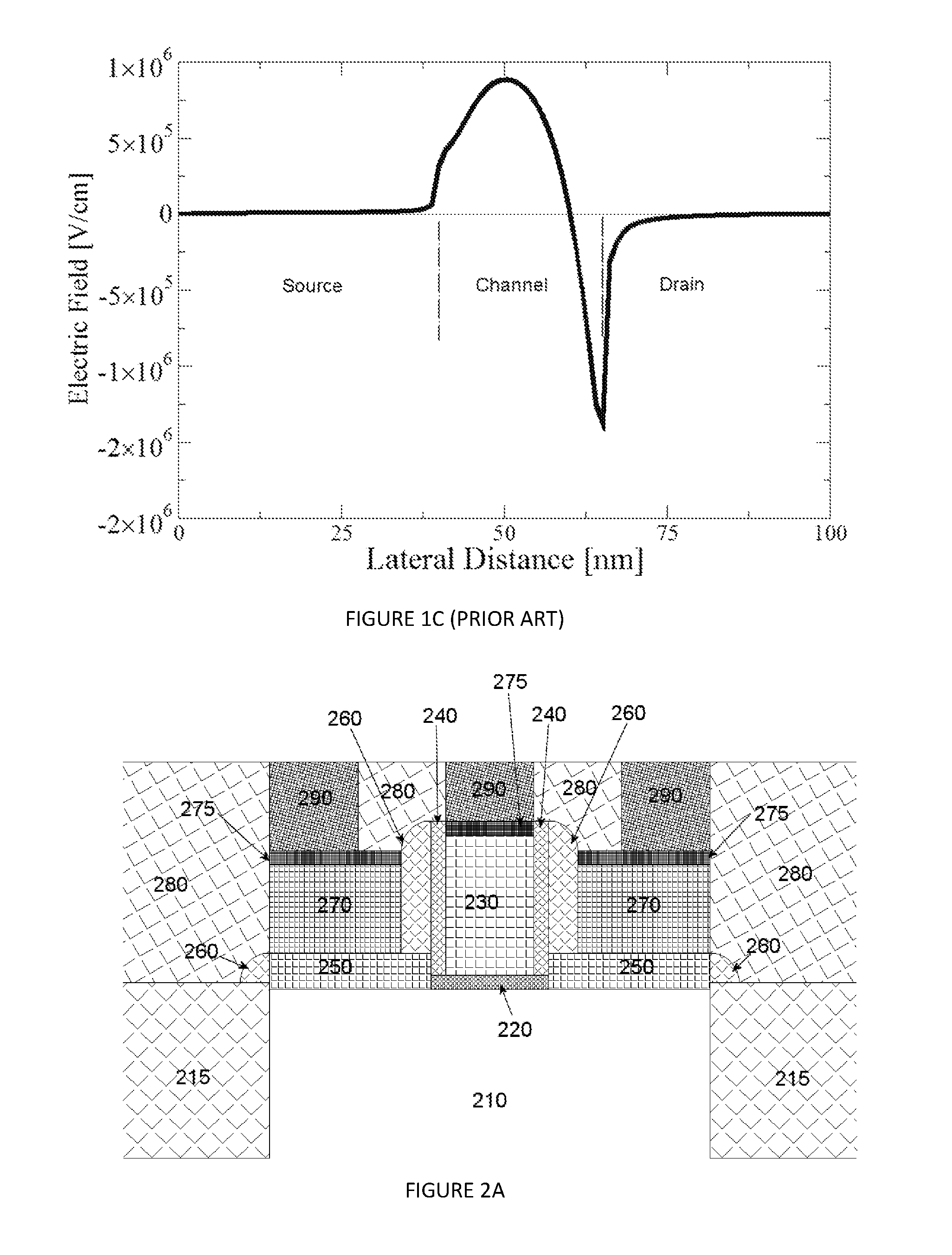
[0048]FIG. 4A shows a gate oxide 420 grown over a well 410 in a semiconductor substrate on which an integrated circuit is to be formed. The region to be occupied by the subject transistor is isolated from other devices by shallow trench isolation regions 415. In general, the well 410 will be doped with acceptors, boron (B) or indium (In) ions, if the subject transistor is to be n-type, or it will be doped with donors, phosphorus (P), arsenic (As) or antimony (Sb), if the subject transistor is to be p-type. In the vicinity of the transistor, doping densities in the range of 1×10¹⁷ to 5×10¹⁸ ions per cm3 are representative, and there is no requirement for extreme doping gradients. In common practice, the gate oxide 420 may be nitrided and a substrate may include one or more oxide thicknesses, as appropriate for the intended operating voltages.

[0049]FIG. 4B shows the result of depositing amorphous or polycrystalline silicon and patterning that material to for a gat...


PUM


Abstract

A device structure with multiple layers of low temperature epitaxy is disclosed that eliminates source and drain and extension implants, providing a planar interface with abrupt junctions between epitaxial extensions and substrate, mitigating electrostatic coupling between transistor drain and transistor channel and reducing short channel effects. The reduction of channel doping results in improved device performance from reduced impurity scattering and reduction of random dopant induced threshold voltage variations (sigma-Vt). Avoiding implants further reduces device sigma-Vt due to random dopants' diffusion from source and drain extensions, which creates device channel length variations during thermal activation anneal of implanted dopants. The defined transistor structure employs at least two levels of low-temperature epitaxy, and creates a planar interface with various types of transistor substrates resulting in performance improvement. Mixed epitaxial layer growth materials inducing tensile or compressive gate stresses can be advantageously used with the invention to further improve device characteristics.

Description

CROSS-REFERENCE TO RELATED APPLICATIONS[0001]This application claims the benefit of U.S. Provisional Patent Application No. 62 / 200,533 filed Aug. 3, 2015.BACKGROUND OF THE INVENTION[0002]1. Field of the Invention[0003]The present invention generally relates to the structure and manufacturing of metal-oxide semiconductor field effect transistors (MOSFETs), and more particularly to MOSFETs manufactured for reproducibility of threshold voltages among otherwise identical transistors and for improvement of transistor performance. Further, this invention addresses random doping induced channel length modulation concerns in transistors manufactured with dimensions finer than 40 nm.[0004]2. Prior Art[0005]Integrated circuits (ICs) have found applications in all areas of human life, like home, health and communications to transportation. The device densities have been doubling every 18 to 24 months and device sizes have been scaling downward to achieve these densities. Currently the most pre...

Claims


Application Information

Patent Timeline
Patent Type & Authority Applications(United States)
IPC IPC(8): H01L29/78
CPCH01L29/7833H01L29/41775H01L29/41783H01L29/665H01L29/66545H01L29/6656H01L29/66628H01L29/7834H01L29/7848H01L29/105H01L29/165
Inventor ASENOV, ASEN
Owner SEMIWISE
Why Eureka
Try Eureka