Resist-pattern-forming method and chemically amplified resist material

a resist material and resist pattern technology, applied in the field of resist pattern forming method and chemically amplified resist material, can solve problems such as hiccups in the practical application of euv lithography

Active Publication Date: 2017-02-23
JSR CORPORATIOON
View PDF19 Cites 15 Cited by
  • Summary
  • Abstract
  • Description
  • Claims
  • Application Information

AI Technical Summary

Benefits of technology

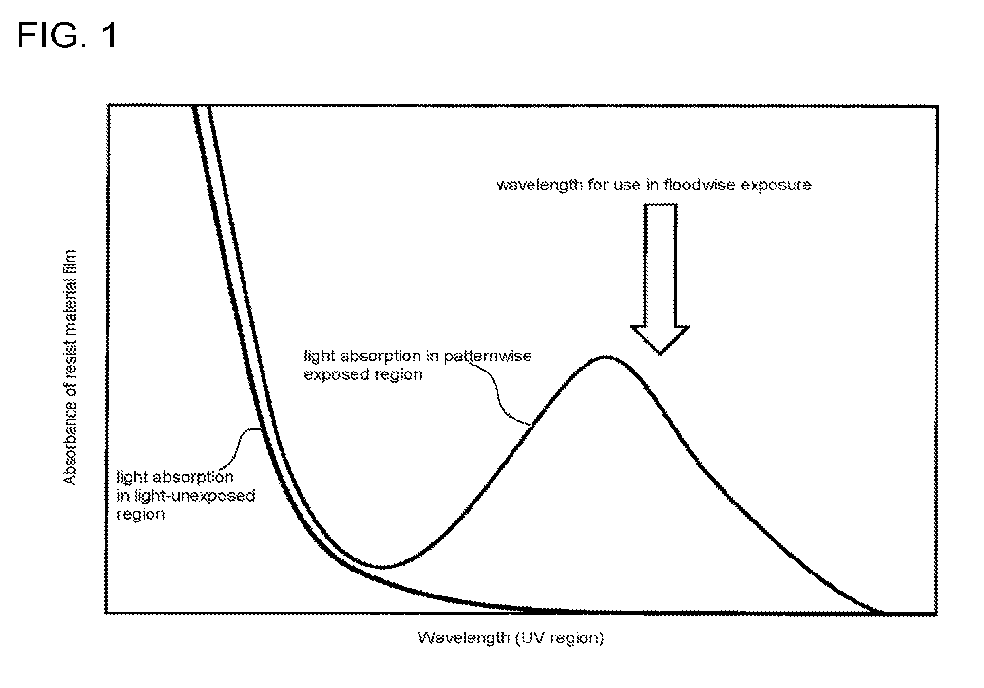
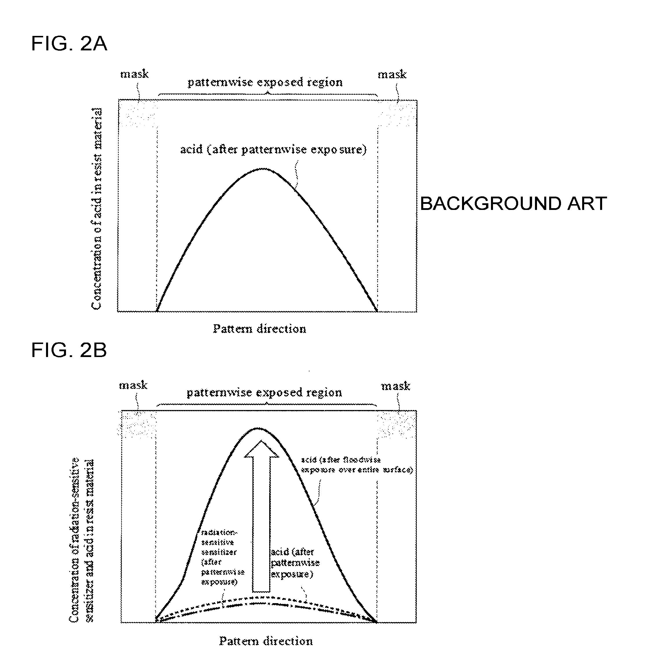
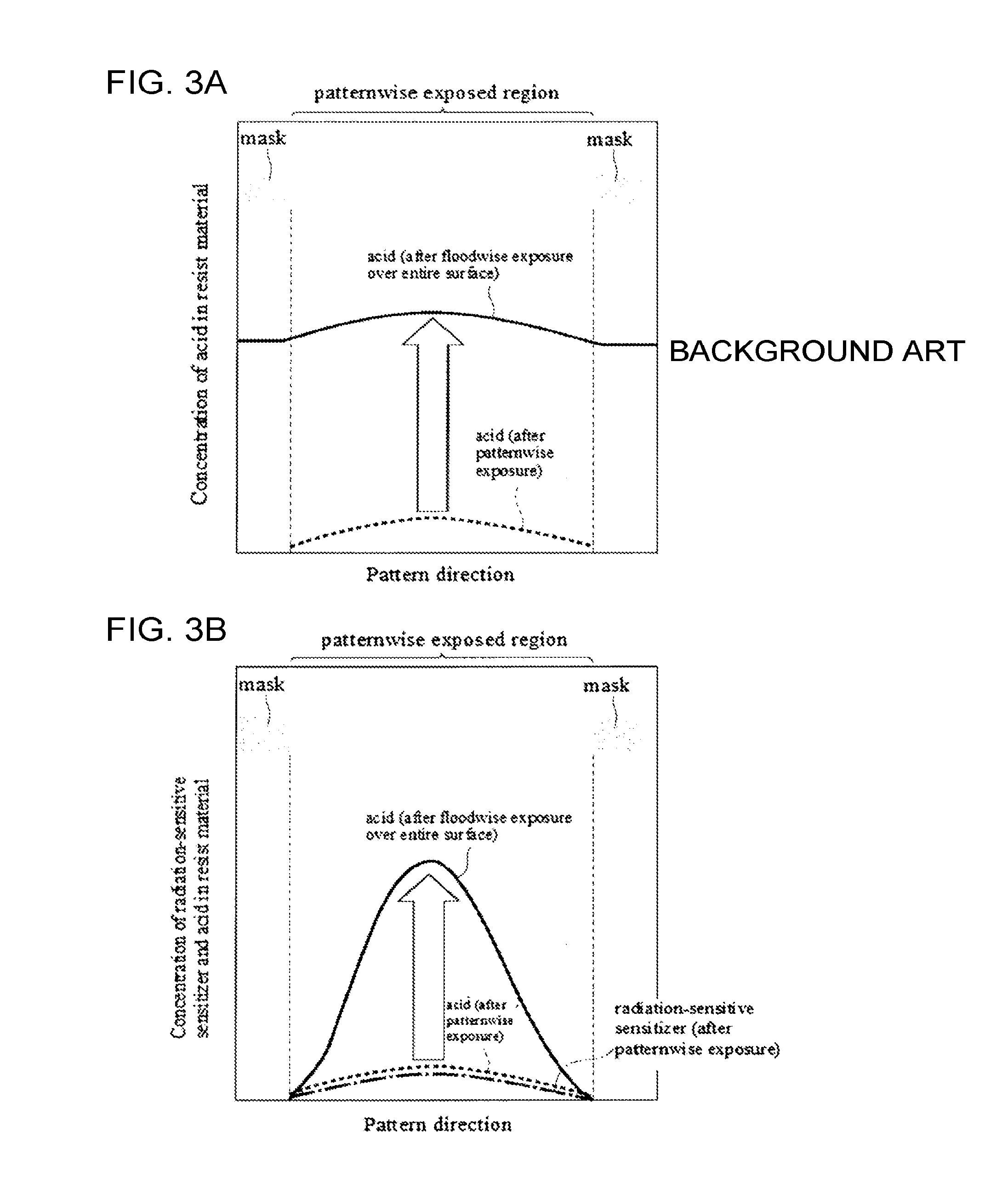
[0007]According to one aspect of the present invention, a resist-pattern-forming method comprises: patternwise exposing a predetermined region of a resist material film made from a photosensitive resin composition comprising a chemically amplified resist material to a first radioactive ray that is ionizing radiation or nonionizing radiation having a wavelength of no greater than 400 nm; floodwise exposing the resist material film patternwise exposed, to a second radioactive ray that is nonionizing radiation having a wavelength greater than the nonionizing radiation for the patternwise exposing and greater than 200 nm; baking the resist material film floodwise exposed; and developing the resist material film baked with a developer solution to form a resist pattern. The chemically amplified resist material comprises: a base component that is capable of being made soluble or insoluble in the developer solution by an action of an acid; and a generative component that is capable of generating a radiation-sensitive sensitizer and an acid upon an exposure. The generative component comprises: a radiation-sensitive acid-and-sensitizer generating agent; any two among the radiation-sensitive acid-and-sensitizer generating agent, a radiation-sensitive sensitizer generating agent, and a radiation-sensitive acid generating agent; or the radiation-sensitive acid-and-sensitizer generating agent, the radiation-sensitive sensitizer generating agent, and the radiation-sensitive acid generating agent. The radiation-sensitive acid-and-sensitizer generating agent generates, upon the exposure to the first radioactive ray, an acid, and a radiation-sensitive sensitizer absorbing the second radioactive ray, and substantially does not generate the acid and the radiation-sensitive sensitizer upon the exposure to the second radioactive ray, in light-unexposed regions that are not exposed to the first radioactive ray in the patternwise exposing. The radiation-sensitive sensitizer generating agent generates, upon the exposure to the first radioactive ray, a radiation-sensitive sensitizer absorbing the second radioactive ray, and substantially does not generate the radiation-sensitive sensitizer upon the exposure to the second radioactive ray, in light-unexposed regions that are not exposed to the first radioactive ray in the patternwise exposing. The radiation-sensitive acid generating agent generates an acid upon the exposure to the first radioactiv

Problems solved by technology

However, since hitherto-developed EUV light sources have low power, the exposure treatment requires a long time period, currently hindering practical application of the

Method used


Image

  • Resist-pattern-forming method and chemically amplified resist material
  • Resist-pattern-forming method and chemically amplified resist material
  • Resist-pattern-forming method and chemically amplified resist material

Examples


synthesis example 1

[0353]55 g (50 mol %) of the compound (M-1), 45 g (50 mol %) of the compound (M-2) and 3 g of azobisisobutyronitrile (AIBN) were dissolved in 300 g of methyl ethyl ketone, followed by polymerizing for 6 hrs under a nitrogen atmosphere while maintaining a reaction temperature at 78° C. Following the polymerization, a reaction solution was added to 2,000 g of methanol dropwise to permit solidification of the polymer. Thereafter, the polymer was washed twice with 300 g of methanol and white powder thus obtained was filtered, followed by drying at 50° C. overnight under a reduced pressure, thereby obtaining a polymer (A-1) served as the base component (1). The polymer (A-1) has the Mw of 7,000 and the Mw / Mn of 2.10. In addition, the result of 13C-NMR analysis indicated that the proportions of the structural units derived from the compound (M-1) and the compound (M-2) were respectively 52 mol % and 48 mol %.

synthesis example 2

[0354]55 g (42 mol %) of the compound (M-3), 45 g (58 mol %) of the compound (M-1), 3 g of AIBN and 1 g of t-dodecyl mercaptan were dissolved in 150 g of propylene glycol monomethyl ether, followed by polymerizing for 16 hrs under a nitrogen atmosphere while maintaining a reaction temperature at 70° C. Following the polymerization, a reaction solution was added to 1,000 g of n-hexane dropwise to permit solidification and purification of a polymer. Subsequently, 150 g of propylene glycol monomethyl ether was added again to the polymer, then 150 g of methanol, 37 g of trimethylamine and 7 g of water were further added thereto, and a hydrolysis reaction was allowed to proceed for 8 hrs with refluxing at the boiling point to permit deacetylation of the structural unit derived from (M-3). After the reaction, the solvent and triethylamine were distilled off under reduced pressure, the resulting polymer was dissolved in 150 g of acetone, and then the solution thus obtained was added to 2,0...

example 1

[0366]The chemically amplified resist material (R-1) was spin-coated onto a silicon wafer in “CLEAN TRACK ACT-8” available from Tokyo Electron Limited, and subjected to PB at 100° C. for 60 sec to form a resist material film having an average thickness of 50 nm. Subsequently, the resist material film was irradiated with an electron beam using a simplified electron beam writer (“HL800D” available from Hitachi, Ltd., power: 50 KeV, current density: 5.0 ampere / cm2) to permit patterning. The patterning was a line and space pattern (1L 1S) obtained by using a mask configured with a line part having a line width of 150 nm and a spaces part formed by neighboring line parts with an interval of 150 nm. After the irradiation with the electron beam for patterning, the following operation (a) or (b) was performed.

Operation (a): Without Floodwise Exposure

[0367]After the irradiation with the electron beam, PEB was carried out at 110° C. for 60 sec in the CLEAN TRACK ACT-8. Then, a development was...


PUM

PropertyMeasurementUnit
Volumeaaaaaaaaaa
Nanoscale particle sizeaaaaaaaaaa

Abstract

A resist-pattern-forming method comprises: patternwise exposing a predetermined region of a resist material film to a first radioactive ray that is ionizing radiation or nonionizing radiation; floodwise exposing the resist material film to a second radioactive ray that is nonionizing radiation; baking the resist material film; and developing the resist material film to form a resist pattern. The resist material film is made from a photosensitive resin composition comprising a chemically amplified resist material. The chemically amplified resist material comprises a base component that is capable of being made soluble or insoluble in a developer solution by an action of an acid and a generative component that is capable of generating a radiation-sensitive sensitizer and an acid upon an exposure. A van der Waals volume of the acid generated from the generative component is no less than 3.0×10⁻²⁸ m3.

Description

CROSS-REFERENCE TO RELATED APPLICATIONS[0001]The present application claims priority to Japanese Patent Application No. 2015-163254, filed Aug. 20, 2015, the contents of which are incorporated herein by reference in their entirety.BACKGROUND OF THE INVENTION[0002]Field of the Invention[0003]The present invention relates to a resist-pattern-forming method and a chemically amplified resist material.[0004]Discussion of the Background[0005]EUV (extreme-ultraviolet) lithography attracts attention as one of element technologies for manufacture of the next generation of semiconductor devices. The EUV lithography is a pattern formation technology in which EUV light having a wavelength of 13.5 nm is utilized as an exposure light. It is demonstrated that the EUV lithography enables an extremely fine pattern (no greater than 20 nm, for example) to be formed in an exposure step of a manufacture process of the semiconductor devices.[0006]However, since hitherto-developed EUV light sources have l...

Claims


Application Information

Patent Timeline
IPC IPC(8): G03F7/20G03F7/32G03F7/039G03F7/38
CPCG03F7/203G03F7/0397G03F7/322G03F7/38C07D409/14C08F220/283G03F7/0045G03F7/0046G03F7/2022G03F7/004G03F7/0382G03F7/0392G03F7/168G03F7/20C07C303/32C07C309/07C07C381/12C08F220/14C08F220/22C08F220/26G03F7/2002H01L21/0274
Inventor NAKAGAWA, HISASHINARUOKA, TAKEHIKONAGAI, TOMOKITAGAWA, SEIICHIOSHIMA, AKIHIRONAGAHARA, SEIJI
Owner JSR CORPORATIOON
Why Eureka
Try Eureka