
Piezoelectric element and piezoelectric element applied device

Active Publication Date: 2017-03-02
SEIKO EPSON CORP
View PDF4 Cites 19 Cited by
  • Summary
  • Abstract
  • Description
  • Claims
  • Application Information

AI Technical Summary

Benefits of technology

This patent describes a method to improve the performance of piezoelectric layers in crystals, such as those used in piezoelectric devices. The method involves controlling the amount of metal in the piezoelectric layer, specifically by ensuring that the ratio of moles of metal to the number of moles of metal in the piezoelectric layer is greater than 80%. This results in improved piezoelectric characteristics and a larger displacement capacity. Additionally, the method also involves separating the peaks in the X-ray diffraction pattern of the piezoelectric layer, which indicates that the layer is tetragonal or orthorhombic, rather than pseudo-cubic, which further improves the piezoelectric performance.

Problems solved by technology

However, in a case where the crystal structure is approximately pseudo-cubic, the crystal structure is unstable in terms of energy, and thus a large displacement amount is easily obtained with a small amount of energy.
However, because the crystal structure has a shape which is close to a cubic crystal which does not indicate ferroelectric properties, in a case where a large amount of energy is applied to the crystal, large displacement is structurally difficult to occur.
Such a problem is not limited to a piezoelectric element used in a piezoelectric actuator which is mounted in a liquid ejecting head represented by an ink jet recording head, and similarly also occurs in a piezoelectric element used in other piezoelectric element applied devices.

Method used


Image

  • Piezoelectric element and piezoelectric element applied device
  • Piezoelectric element and piezoelectric element applied device
  • Piezoelectric element and piezoelectric element applied device

Examples


embodiment 1

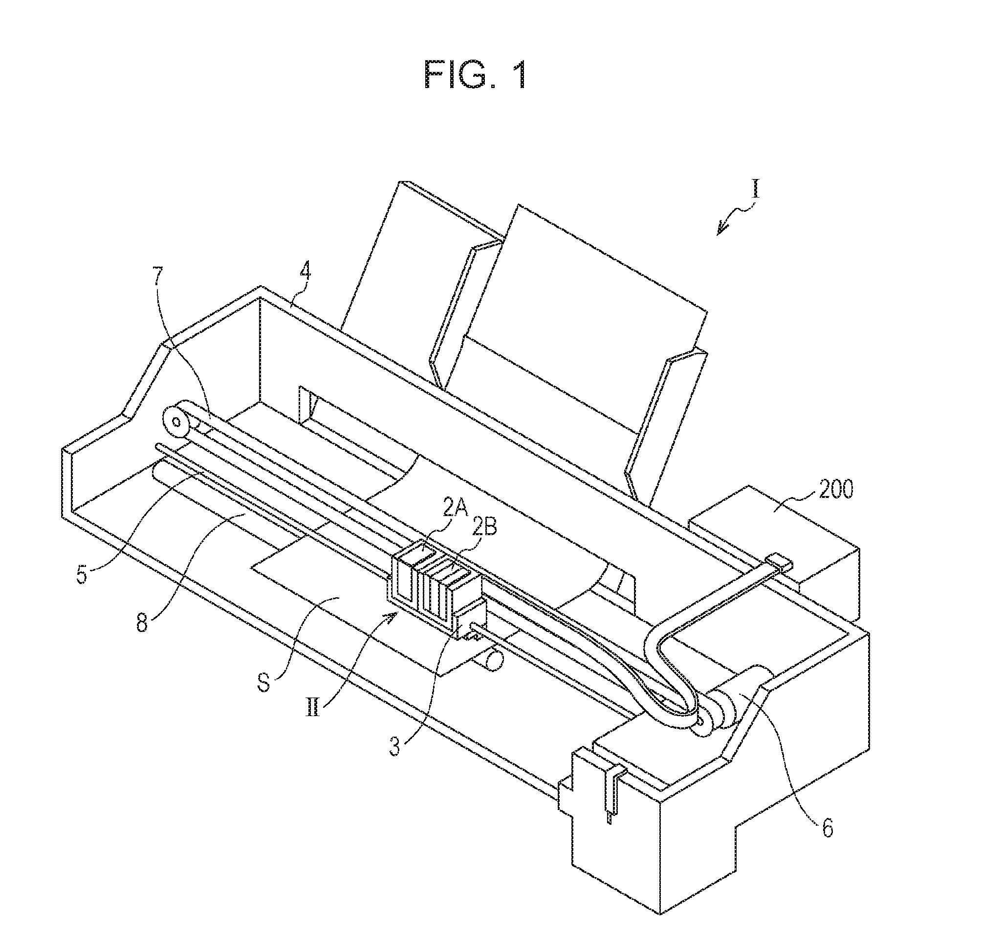
[0042]FIG. 1 illustrates an ink jet type recording apparatus which is an example of a liquid ejecting apparatus. The liquid ejecting apparatus includes a recording head which is an example of a piezoelectric element applied device according to an embodiment of the invention. As illustrated in FIG. 1, in an ink jet type recording apparatus I, an ink jet recording head unit (head unit) II which includes a plurality of ink jet recording heads is provided so as to be attachable to cartridges 2A and 2B. The cartridges 2A and 2B constitute an ink supply section. A carriage 3 having the head unit II mounted therein is provided with a carriage shaft 5 so as to be movable in a shaft direction. The carriage shaft 5 is attached to a main body 4 of the apparatus. For example, the carriage 3 has a function of discharging a black ink composition and a color ink composition.

[0043]A driving force of a driving motor 6 is transferred to the carriage 3 through a plurality of gears and timing belts 7 (...

example 1

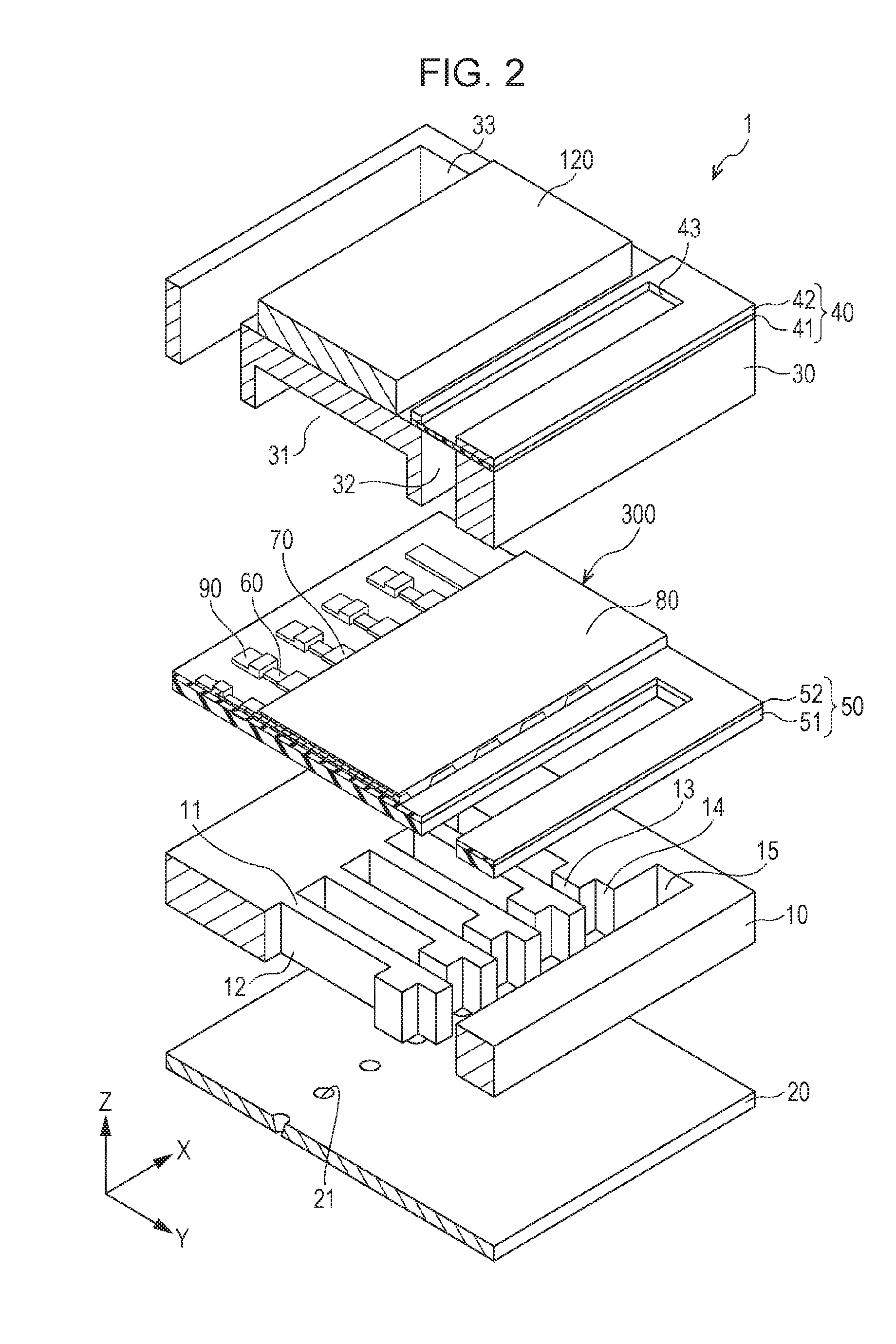
[0087]A surface of a silicon substrate which is used as the passage formation substrate 10 was thermally oxidized, and thus the elastic film 51 formed from silicon dioxide was formed on the silicon substrate. Then, a zirconium film was formed on the elastic film 51 by sputtering, and the zirconium film was thermally oxidized. Thus, the insulating film 52 formed from zirconium oxide was formed. Then, a titanium film was formed on the insulating film 52 by sputtering, thereby forming the adhesive layer 56. After a platinum film was formed on the adhesive layer 56 by using a sputtering method, the platinum film was patterned so as to have a predetermined shape. Thus, the first electrode 60 having a thickness of 50 nm was formed.

[0088]Then, the piezoelectric layer 70 was formed through the following procedures. Firstly, an n-octane solution of potassium acetate, an n-octane solution of sodium acetate, and an n-octane solution of pentaethoxy niobium were mixed, thereby preparing a precur...

example 2

[0101]Example 2 has the premise of a crystal phase other than the pseudo-cubic crystal in a case where a KNN-based piezoelectric body is thinned. Example 2 has a purpose for improving variability characteristics by sufficiently using movement of domains. In Example 2, the dielectric constant is set to be high in a low temperature range, and piezoelectric characteristics are improved.

[0102]Firstly, similarly to Example 1, the elastic film 51, the insulating film 52, the adhesive layer 56, and the first electrode 60 were formed on the substrate 10.

[0103]Then, the piezoelectric layer 70 was formed by the following procedures.

[0104]Firstly, a solution formed from potassium 2-ethylhexanoate, sodium 2-ethyl hexanoate, niobium 2-ethylhexanoate, and manganese 2-ethylhexanoate was prepared. Mixing for a precursor solution was performed by using the prepared solution, so as to have the following composition. (K0.4Na0.6)(Nb0.995Mn0.005)O3

[0105]The precursor solution is applied on the substrat...


PUM


Abstract

A piezoelectric element includes a first electrode, a piezoelectric layer which is formed on the first electrode by using a solution method, and is formed from compound oxide which has a perovskite structure in which potassium, sodium, and niobium are provided, and a second electrode which is provided on the piezoelectric layer. The piezoelectric layer has a peak derived from a (200) plane and a peak derived from a (002) plane in an X-ray diffraction pattern obtained by θ−2θ measurement.

Description

BACKGROUND[0001]1. Technical Field[0002]The present invention relates to a piezoelectric element which includes a first electrode, a piezoelectric layer, and a second electrode, and a piezoelectric element applied device which includes the piezoelectric element.[0003]2. Related Art[0004]Generally, a piezoelectric element includes a piezoelectric layer and two electrodes. The piezoelectric layer has electromechanical conversion characteristics. The piezoelectric layer is interposed between the two electrodes. A device (piezoelectric element applied device) which uses such a piezoelectric element as a driving source has recently been actively developed. As one of the piezoelectric element applied devices, for example, a liquid ejecting head represented by an ink jet recording head, a MEMS element represented by a piezoelectric MEMS element, an ultrasonic measurement device represented by an ultrasonic sensor and the like, and a piezoelectric actuator device are provided.[0005]As a mat...

Claims


Application Information

Patent Timeline
IPC IPC(8): H01L41/187H01L41/047
CPCH01L41/0472H01L41/1873B41J2/045H10N30/2047H10N30/8542B41J2/14233B41J2/161B41J2/1628B41J2/1629B41J2/1632B41J2002/14241H10N30/078
Inventor SAKAI, TOMOHIROSUMI, KOJIISSHIKI, TETSUYATAKAHASHI, TOSHIAKIKOBAYASHI, TOMOKAZUKITADA, KAZUYA
Owner SEIKO EPSON CORP
Learn More