Semiconductor device or electronic device including the semiconductor device

a semiconductor and electronic technology, applied in pulse generators, pulse techniques, instruments, etc., can solve the problems of increasing power consumption and other problems, and achieve the effect of reducing circuit size, reducing power consumption and efficiently compressing data

Inactive Publication Date: 2017-03-02
SEMICON ENERGY LAB CO LTD
View PDF2 Cites 52 Cited by
  • Summary
  • Abstract
  • Description
  • Claims
  • Application Information

AI Technical Summary

Benefits of technology

[0029]According to one embodiment of the present invention, a novel semiconductor device having a learning function, a pattern recognition function, or the like. According to one embodiment of the present invention, a novel semiconductor device with a decreased circuit size. According to one embodiment of the present invention, a novel sem...

Problems solved by technology

Furthermore, since refresh operation of analog data i...

Method used


Image

  • Semiconductor device or electronic device including the semiconductor device
  • Semiconductor device or electronic device including the semiconductor device
  • Semiconductor device or electronic device including the semiconductor device

Examples


embodiment 1

[0076]In this embodiment, an example of a semiconductor device according to the disclosed invention will be described.

Structure Example

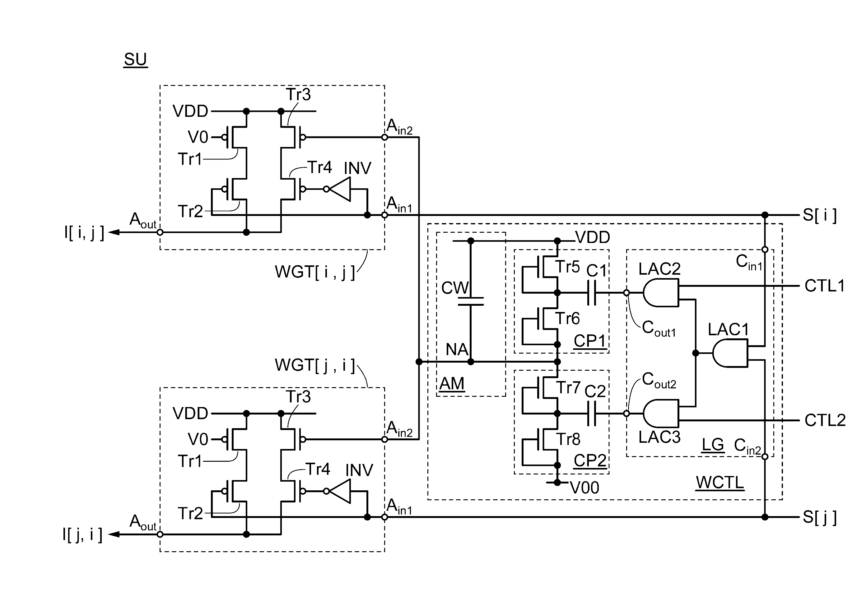
[0077]FIG. 3 illustrates a semiconductor device of one embodiment of the present invention. A semiconductor device 100 includes neuron circuits NU[1] to NU[n] and (n2−n) synapse circuits SU (n is an integer of 2 or more).

[0078]The synapse circuits SU are arranged so that n circuits are arranged per side. In FIG. 3, the synapse circuit SU in an i-th row and a j-th column is denoted by SU[i, j]. Note that i is an integer of 1 or more and n or less, and j is an integer of 1 or more and n or less. The synapse circuit SU is not provided at the address [i, j] that satisfies i=j. Accordingly, the number of synapse circuits SU included in the semiconductor device 100 is (n2−n).

[0079]The neuron circuit NU[1] is electrically connected to the synapse circuits SU[2, 1] to SU[n, 1] in the first column and the synapse circuits SU[1, 2] to SU[1, n] in the first row...

operation example

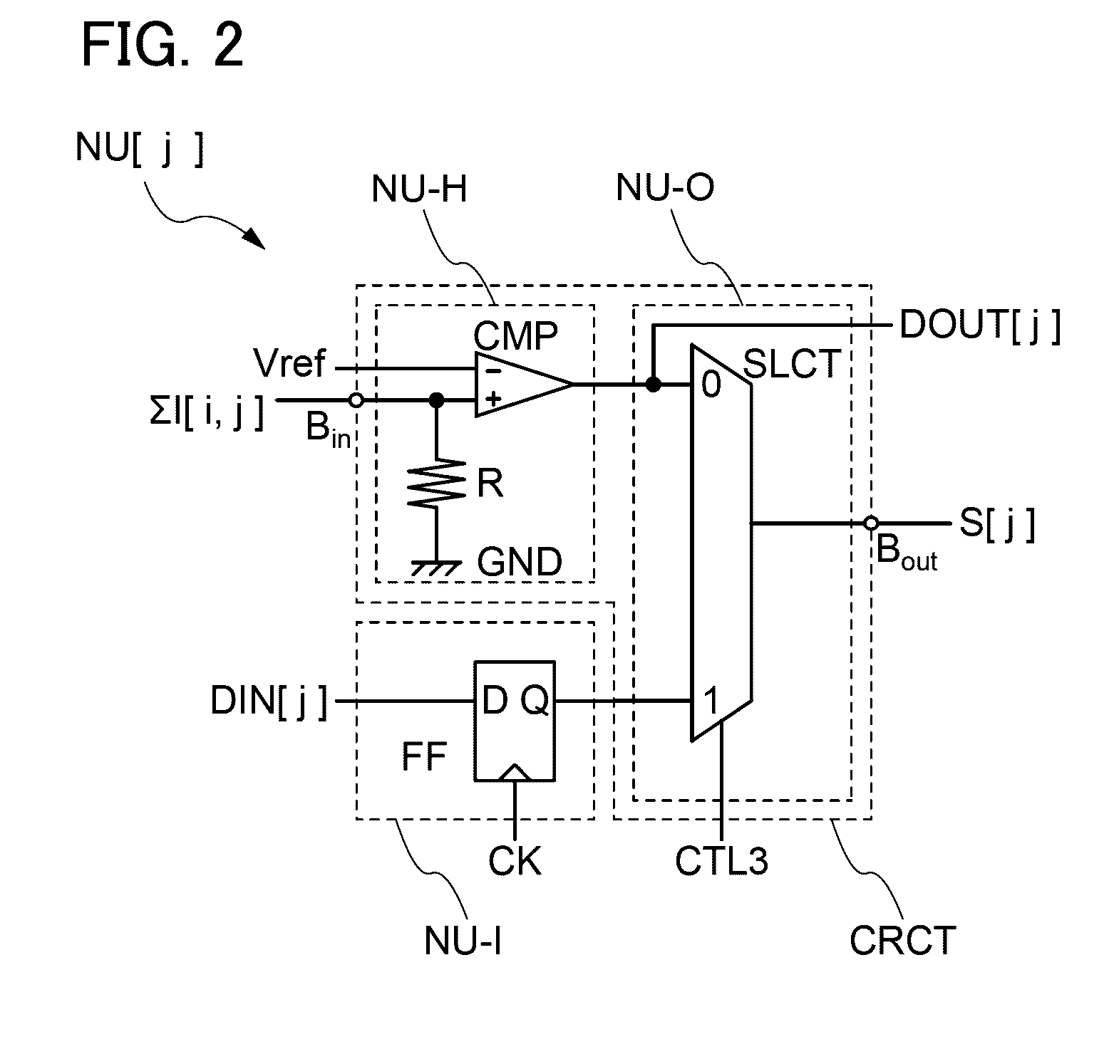
[0177]Here, an operation example of the semiconductor device 100 is described. The operation here refers to operation in which learning data is input to the semiconductor device 100 so that the semiconductor device 100 learns the learning data, object data is input to the semiconductor device 100, and judgment whether the learning data and the object data match, are similar, or mismatch is made. FIG. 10 and FIG. 11 are flowcharts of the operation of the semiconductor device 100. Note that the operation example of the semiconductor device 100 including the neuron circuit NU[i] illustrated in FIG. 2 and the synapse circuit SU illustrated in FIG. 1 is described here.

>

[0178]First, operation where the semiconductor device 100 learns data is described with reference to FIG. 10.

[Step S1-1]

[0179]In Step S1-1, learning data is input from the outside to the neuron circuit NU. Note that leaning data is represented in binary here, and the number of neuron circuits to which learning data is inpu...

embodiment 2

[0208]In this embodiment, an operation example of the case where the semiconductor device 100 described in Embodiment 1 is used as an encoder is described.

>

[0209]First, an example of a method for detecting an object motion is described. FIGS. 12A to 12F illustrate an algorithm that the semiconductor device 100 performs for detection of an object motion in image data.

[0210]FIG. 12A shows image data 10 that has a triangle 11 and a circle 12. FIG. 12B shows image data 20 where the triangle 11 and the circle 12 of the image data 10 are moved to the upper right.

[0211]Image data 30 in FIG. 12C shows operation by which a region 31 including the triangle 11 and the circle 12 is extracted from the image data 10. In the image data 30, a cell at the upper left corner of the extracted region 31 is regarded as a reference point (0, 0), and numbers indicating positions in the right / left direction and the upper / lower direction are added to the image data 10. The extracted region 31 of FIG. 12C is ...


PUM


Abstract

To provide a semiconductor device with a small circuit size and low power consumption or an electronic device including the semiconductor device and compressing a large volume of image data. A semiconductor device of a Hopfield neural network is formed using neuron circuits and synapse circuits. The synapse circuit includes an analog memory and a writing control circuit, and the writing control circuit is formed using a transistor including an oxide semiconductor in a channel formation region. Thus, data retention lifetime of the analog memory can be extended and refresh operation for data retention can be omitted, so that power consumption of the semiconductor device can be reduced. The semiconductor device enables judgement whether learned image data and arbitrary image data match, are similar, or mismatch by comparing video data. Thus, motion compensation prediction, which is one of data compression methods, can be employed for image data.

Description

TECHNICAL FIELD[0001]One embodiment of the present invention relates to a semiconductor device or an electronic device including the semiconductor device.[0002]Note that one embodiment of the present invention is not limited to the above technical field. The technical field of the invention disclosed in this specification and the like relates to an object, a method, or a manufacturing method. Another embodiment of the present invention relates to a process, a machine, manufacture, or a composition of matter. Specifically, examples of the technical field of one embodiment of the present invention disclosed in this specification include a semiconductor device, a display device, a liquid crystal display device, a light-emitting device, a power storage device, an imaging device, a memory device, a processor, a converter, an encoder, a decoder, a tuner, an electronic device, a method for driving any of them, a method for manufacturing any of them, a method for testing any of them, and a ...

Claims


Application Information

Patent Timeline
IPC IPC(8): H03K3/356H02M3/07H04N19/42H01L29/786
CPCH03K3/356104H04N19/42H02M3/07H01L29/7869H01L29/78648H01L29/78696H01L27/1225H04N19/43G06N3/08G06N3/049G06N3/065G06N3/044
Inventor KUROKAWA, YOSHIYUKI
Owner SEMICON ENERGY LAB CO LTD
Why Eureka
Try Eureka