Process for the production of two-dimensional nanomaterials

a two-dimensional nanomaterial and nanotechnology, applied in single-layer graphene, boron compounds, coatings, etc., can solve the problems of large area, long synthesis time, and unyielding problem of single crystal graphene with a controlled number of layers, so as to reduce the influence of any topographic defects, reduce the number of layers, and reduce the effect of synthesis kinetics

Active Publication Date: 2017-04-27
OXFORD UNIV INNOVATION LTD
View PDF1 Cites 14 Cited by
  • Summary
  • Abstract
  • Description
  • Claims
  • Application Information

AI Technical Summary

Benefits of technology

[0009]The processes and substrates of the present invention may be advantageous in a number of respects. For instance, by employing a material which forms a liquid surface on the substrate, it may be possible to minimise the influence of any topographic defects on the quality of the resulting two-dimensional nanomaterials. In addition, since the lattice of the substrate will be substantially screened by the liquid surface, the two-dimensional nanomaterial may be allowed to grow in its natural shape (e.g. graphene may be allowed to grow in its natural hexagonal shape). The chemical kinetics of the synthesis may also be changed. Thus, two-dimensional nanomaterials produced by the present processes may exhibit low nucleation density and high growth rates, allowing millimeter-sized flakes to grow easily in short time periods compared to methods which do not utilise a liquid surface on the substrate. Moreover, conventional substrate preparation steps (e.g. polishing, chemical and / or electrochemical etching, or long annealing) may be largely obviated.

Problems solved by technology

Notably, the production of large area, single crystal graphene with a controlled number of layers has been an unyielding problem.
The synthesis time is thus lengthy and significant quantities of source materials must be used.
However, these methods are time and energy consuming, and thus costly.
Alternatively, expensive single crystal substrates of limited size have been used, but such substrates cannot be upscaled.

Method used


Image

  • Process for the production of two-dimensional nanomaterials
  • Process for the production of two-dimensional nanomaterials
  • Process for the production of two-dimensional nanomaterials

Examples


example 1

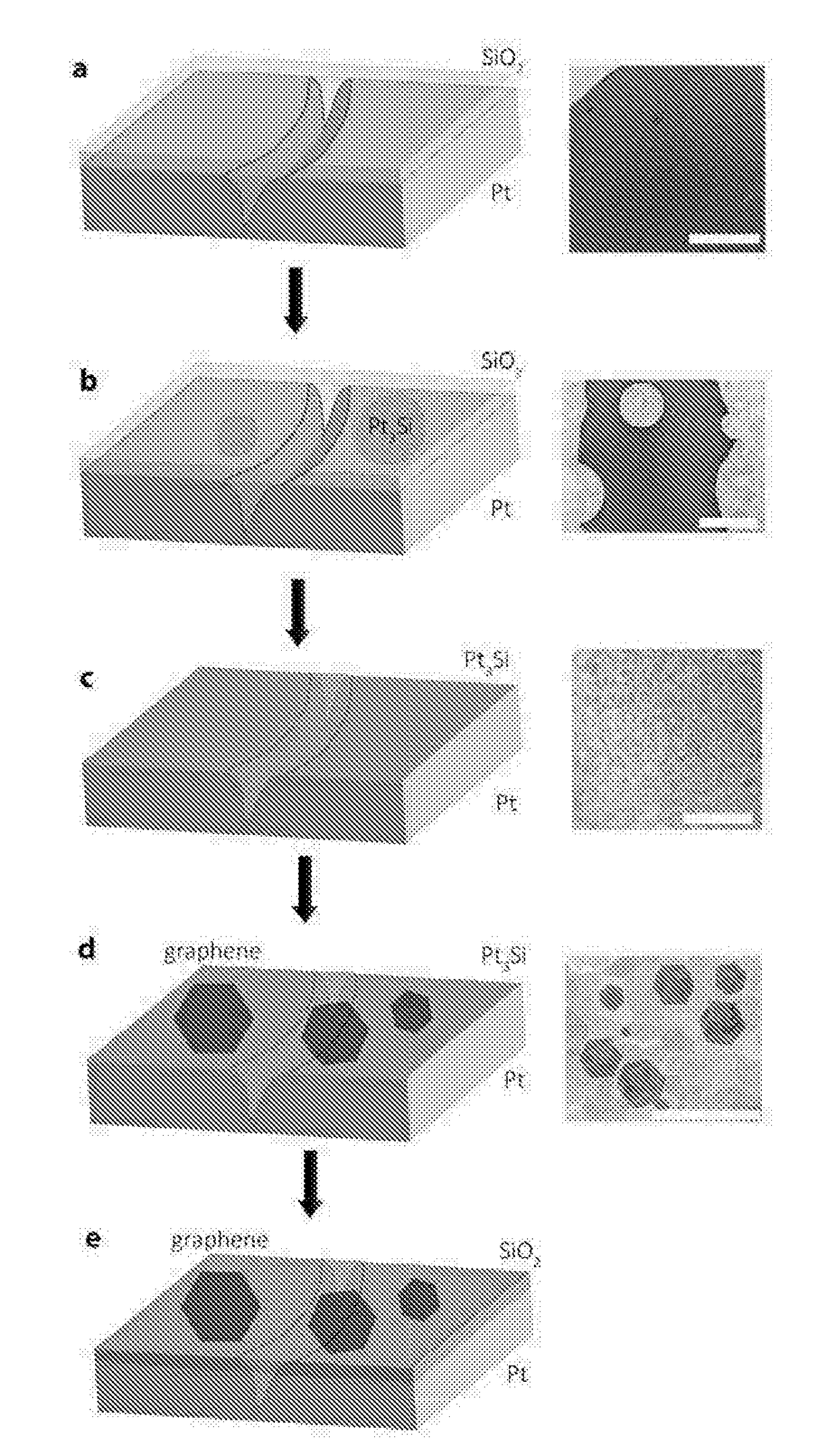
[0054]The following Example illustrates a process for the production of graphene using a silicidated platinum substrate.

Materials and Methods

Substrate Preparation

[0055]A film of SiO2 of specified thickness was deposited onto a 25 μm thick Pt foil (Goodfellow, 99.95% purity, washed in acetone and deionized water) via CVD with a tetraethyl orthosilicate (TEOS) precursor. For example, a SiO2 film of about 1 μm thickness can be deposited on clean Pt with CVD by passing Ar gas (350 sccm) through a TEOS precursor at about 700° C. for 30 minutes. Other methods, such as Si, SiO, SiO2 evaporation, sputtering and sol-gel processes can also be used to deposit the film onto the foil.

Graphene Synthesis

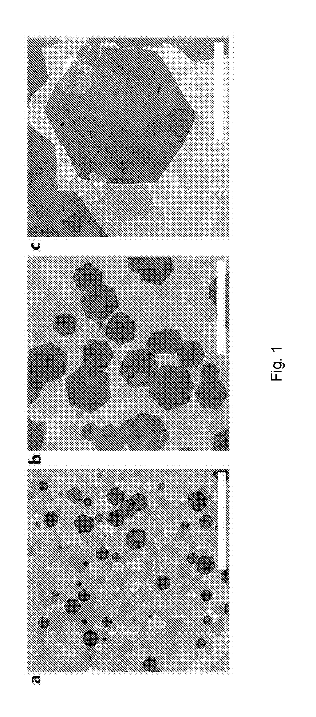
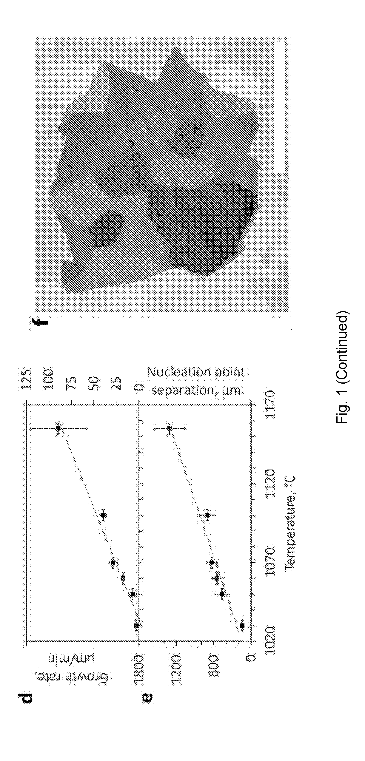
[0056]Graphene was synthesised in a standard CVD apparatus at atmospheric pressure with a methane (CH4) and hydrogen (H2) gas mixture. The CVD apparatus consisted of a gas system with three gases: CH4, H2, Ar (99.995% purity), controlled with mass flow controllers. The outlet line with the gas mixt...

example 2

[0070]Following similar procedures, hexagonal flakes of monolayer graphene can be grown on silicidated palladium foils. By way of illustration, hexagonal monolayer graphene flakes of about 300 μm size with about 3 mm nucleation point separation can be achieved by depositing a 50 nm SiO2 layer, followed by annealing at 1150° C. with hydrogen flow of 200 sccm for 30 minutes, followed by a 15 minute synthesis stage with 1.8 sccm methane and 600 sccm hydrogen.

example 3

[0071]Moreover, similar procedures may be used to grow hexagonal boron nitride on silicidated platinum. By way of illustration, a SiO2 film of about 1 μm is deposited on pristine Pt with CVD by passing Ar gas (350 sccm) through a TEOS precursor at about 700° C. The substrate is annealed under 200 sccm hydrogen flow for 30 minutes at 1070° C. to form the silicide. Hexagonal boron nitride is then grown by CVD. The vapour of ammonia borane precursor (100 mg in a quartz container, heated to around 100° C.) is carried by a 10 sccm flow of hydrogen, this flow is then diluted with 200 sccm of hydrogen in a quartz tube. The flow through the quartz tube enters a furnace heated to 1000° C. with the hot silicidated Pt substrate. The synthesis time is 30 minutes, after which the substrate is quenched by moving the furnace away from the substrate.


PUM

PropertyMeasurementUnit
thicknessaaaaaaaaaa
thicknessaaaaaaaaaa
thicknessaaaaaaaaaa

Abstract

The present invention provides a process for producing a two-dimensional nanomaterial, the process comprising forming the two-dimensional nanomaterial on a surface of a substrate by CVD, wherein said surface is a liquid surface which comprises a molten eutectic compound. Substrates and substrate precursors for use in said process are also provided.

Description

[0001]The work leading to this invention has received funding from the European Community's Seventh Framework Programme (FP7 / 2007-2013) under grant agreement no. 240500.FIELD OF THE INVENTION[0002]This invention relates to the production of two-dimensional nanomaterials by chemical vapour deposition (CVD). In particular, the invention relates to processes and substrates for the production of graphene and other two-dimensional nanomaterials by CVD.BACKGROUND TO THE INVENTION[0003]Superior quality graphene is highly sought in modern research due to the many desirable properties that it possesses. Graphene is a promising candidate for use in a wide variety of applications such as transparent flexible electrodes, photonic devices, energy storage, gas sensors and filters, transistors, coatings and solar energy and many more. Exceptional electrical, optical and mechanical properties of the material depend greatly on the quality of the synthesised graphene and the underlying substrate. Not...

Claims


Application Information

Patent Timeline
Patent Type & Authority Applications(United States)
IPC IPC(8): C23C16/00C23C16/34C01B21/064C23C16/40C23C16/01C23C16/44C23C16/26C23C16/30
CPCC23C16/003C23C16/26C23C16/342C23C16/305C23C16/40C23C16/01Y10S977/843C01B31/0453C01B21/064C01B2204/02B82Y40/00B82Y30/00Y10S977/734C23C16/44C01B21/0646C01B32/186C01B35/08
Inventor BABENKO, VITALIYGROBERT, NICOLE
Owner OXFORD UNIV INNOVATION LTD
Why Eureka
Try Eureka