Electroluminescent device

a technology of electroluminescent devices and el, which is applied in the direction of basic electric elements, semiconductor devices, electrical equipment, etc., can solve the problems of optical out-coupling of oled internal emission to air, and achieve the effect of high optical out-coupling efficiency and external quantum efficiency

Inactive Publication Date: 2017-05-04
NAT TAIWAN UNIV
View PDF3 Cites 5 Cited by
  • Summary
  • Abstract
  • Description
  • Claims
  • Application Information

AI Technical Summary

Benefits of technology

[0007]Researches reveal that emitters having preferential in-plane (horizontal) emitting dipoles are beneficial to optical out-coupling (light extraction) of OLEDs using the conventional high-refractive-index transparent electrode ITO, since the number (ratio) of vertical emitting dipoles contributing little to external emission is reduced and the radiation pattern of a horizontal emitting dipole is in general more suitable for optical out-coupling.
[0008]Here this invention discloses that by combining the emitters having preferential in-plane (horizontal) emitting dipoles, the low-refractive-index transparent electrode, and a substrate or superstrate with an optical out-coupling treatment in an organic electroluminescent device, improved and very high optical out-coupling efficiency and external quantum efficiency can be achieved.

Problems solved by technology

However, in typical OLED structures, the optical out-coupling of OLED internal emission to air is an issue for achieving high external quantum efficiencies.
Thus, due to the significant refractive-index mismatches at air / substrate and substrate / ITO interfaces in typical OLEDs, OLED internal emission usually suffers total internal reflection and hence most of internal radiation is trapped and guided inside the device.

Method used


Image

  • Electroluminescent device
  • Electroluminescent device
  • Electroluminescent device

Examples


embodiment of invention — example 1

Embodiment of Invention—Example 1

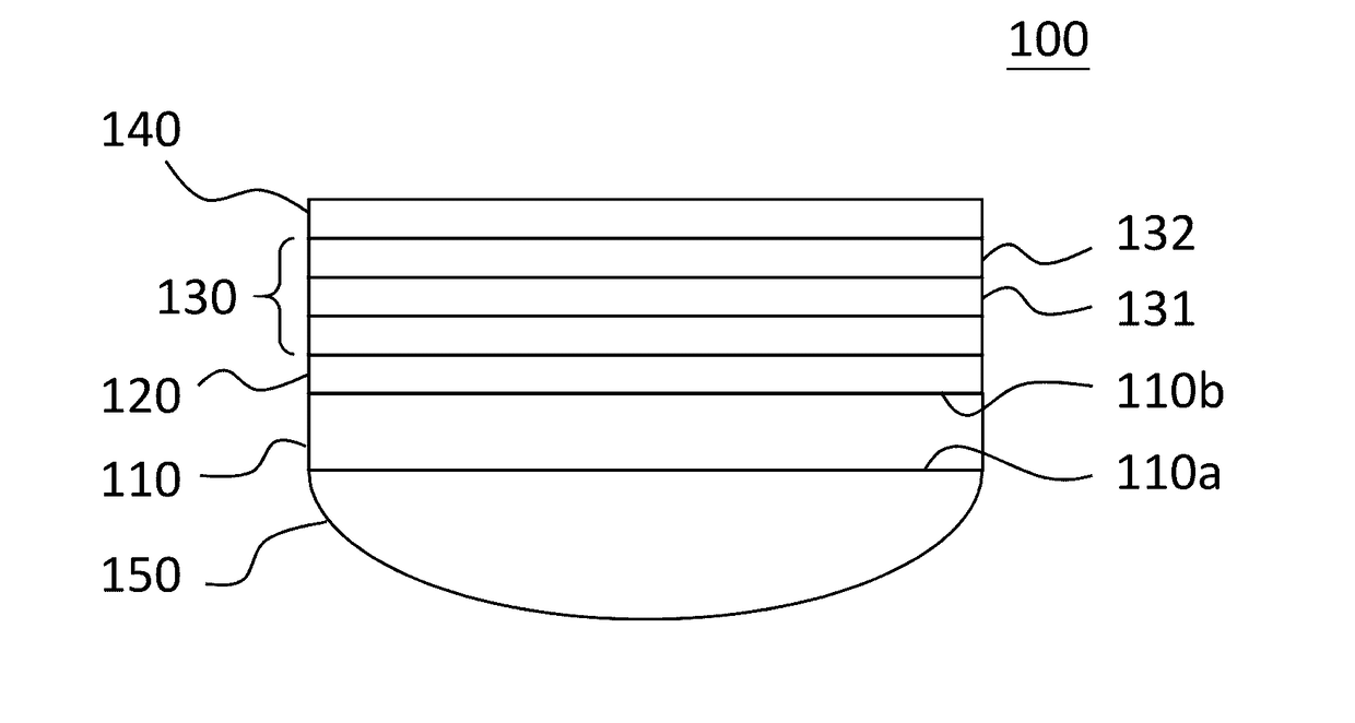
[0044]In one possible embodiment of this invention, the low-index transparent electrode (the first electrode) could be a transparent conducting polymer poly(3,4-ethylenedioxythiophene):poly(styrenesulfonate) (PEDOT:PSS) with sufficient conductivity. The conducting polymer poly(3,4-ethylenedioxythiophene):poly(styrenesulfonate) (PEDOT:PSS) has been attractive due to its excellent mechanical flexibility, good transmittance and conductivity, solution processing capability, and low cost. With a conductivity almost comparable to that of ITO, high-conductivity PEDOT:PSS can be used as transparent electrodes for organic optoelectronic devices. PEDOT:PSS possesses optical properties (e.g., refractive index, n˜1.5) rather different from those of the widely used transparent conductor ITO (n˜1.9-2.1) and typical organic layers (n˜1.7-1.9).

[0045]Here, we conducted comprehensive theoretical and experimental comparisons on OLEDs adopting either the conventional hi...

embodiment of invention — example 2

Embodiment of Invention—Example 2

[0063]Following the general principles of the preceding embodiment example, there could be different variations and modifications of the embodiment.

[0064]For instance, in addition to the low-index transparent electrode PEDOT:PSS in example 1, other possible low-index transparent conductors (preferentially with a refractive index <1.7) include nanoporous indium tin oxide, nanoporous fluorine-doped tin oxide, nanoporous aluminum zinc oxide, nanoporous gallium zinc oxide, nanoporous tin oxide, nanoporous niobium-doped titanium oxide, their combinations, and their stacking.

embodiment of invention — example 3

Embodiment of Invention—Example 3

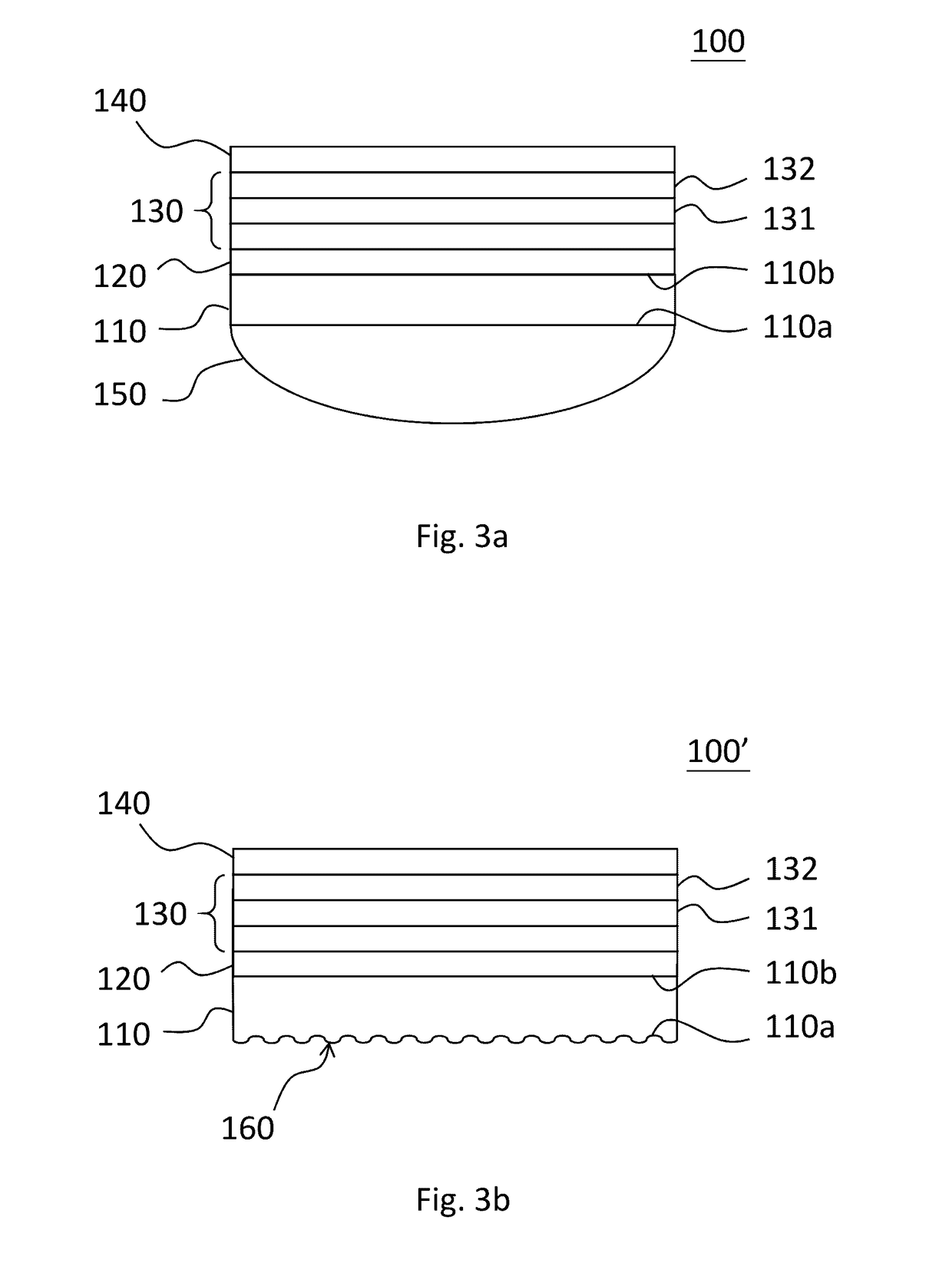
[0065]For instance, the out-coupling lens attached to the substrate in example 1 may be replaced with other out-coupling optical element adjacent to the outer surface of the substrate, such as a prism, a pyramid, a hemisphere lens, a macrolens sheet, a microlens sheet, a micro-prism sheet, a micro-pyramid sheet, a micro-particle layer, a nano-particle layer, a microporous layer, a nanoporous layer, a grating sheet, a scattering sheet, a diffuser sheet, arrays of pores, arrays of crevices, arrays of air bubbles, arrays of vacuum pores etc.


PUM


Abstract

An electroluminescent device is provided. The electroluminescent device includes a substrate or superstrate, an optical out-coupling structure, a first electrode, a functional stack, and a second electrode. The substrate has an outer surface and an opposite inner surface. The optical out-coupling structure situates on the outer surface. The first electrode is disposed on the inner surface. The first electrode is transparent and has a refractive index equal to or less than 1.7. The functional stack is disposed on the first electrode and includes a light emitting layer. The light emitting layer contains an emitting material having preferential horizontal emitting dipoles with a horizontal dipole ratio being equal to or larger than 70%. The second electrode is disposed on the functional stack.

Description

CROSS-REFERENCE TO RELATED APPLICATION[0001]This application claims priority to and the benefit of U.S. Provisional Patent Application Ser. No. 62 / 285,462, filed on Oct. 30, 2015, and entitled “Electroluminescent devices with high optical out-coupling efficiencies”, the disclosure of which is incorporated by reference in its entirety.FIELD OF THE INVENTION[0002]The present invention pertains to an electroluminescent (EL) device, and more particularly pertains to an organic light-emitting device (OLED) structures with improved optical out-coupling, external quantum efficiencies and their applications.BACKGROUND OF THE INVENTION[0003]Since the reports of efficient and practical organic light-emitting device (OLEDs) in 1987 by Tang and VanSlyke, OLEDs have been subjects of intensive studies and development for displays and lighting applications.[0004]Please refer to FIG. 1, which shows a schematic structure of a known OLED. A typical OLED has an organic layer(s) sandwiched between one ...

Claims


Application Information

Patent Timeline
Patent Type & Authority Applications(United States)
IPC IPC(8): H01L51/52
CPCH01L51/5203H01L51/5262H10K50/11H10K50/81H10K50/828H10K50/858H10K85/1135H10K85/342H10K2102/351H10K50/85H10K50/805
Inventor WU, CHUNG-CHIHLU, CHUN-YANGLEE, WEI-KAIJIAO, MIN
Owner NAT TAIWAN UNIV
Why Eureka
Try Eureka