Background memory test apparatus and methods

a technology of background memory and test apparatus, which is applied in the direction of instruments, coding, code conversion, etc., can solve the problems of increasing the probability of finding such errors quickly, deteriorating memory block typically, but not always, and going undetected

Active Publication Date: 2017-05-11
TEXAS INSTR INC
View PDF16 Cites 16 Cited by
  • Summary
  • Abstract
  • Description
  • Claims
  • Application Information

AI Technical Summary

Benefits of technology

[0020]The schedulable memory scrubbing circuit reads from each address of selected memory blocks with a selected periodicity as determined by a memory test scheduler. The disclosed technique relies on memory controller-impleme

Problems solved by technology

Two errors in a data word results in the latter word being read with the configured parity state and would thus go undetected.
A block of deteriorating memory typically, but not always, exhibits increasing numbers of bad (e.g., “stuck”) bits with the passage of time.
Consequently, the more frequently a particular memory

Method used


Image

  • Background memory test apparatus and methods
  • Background memory test apparatus and methods
  • Background memory test apparatus and methods

Examples


Embodiment Construction

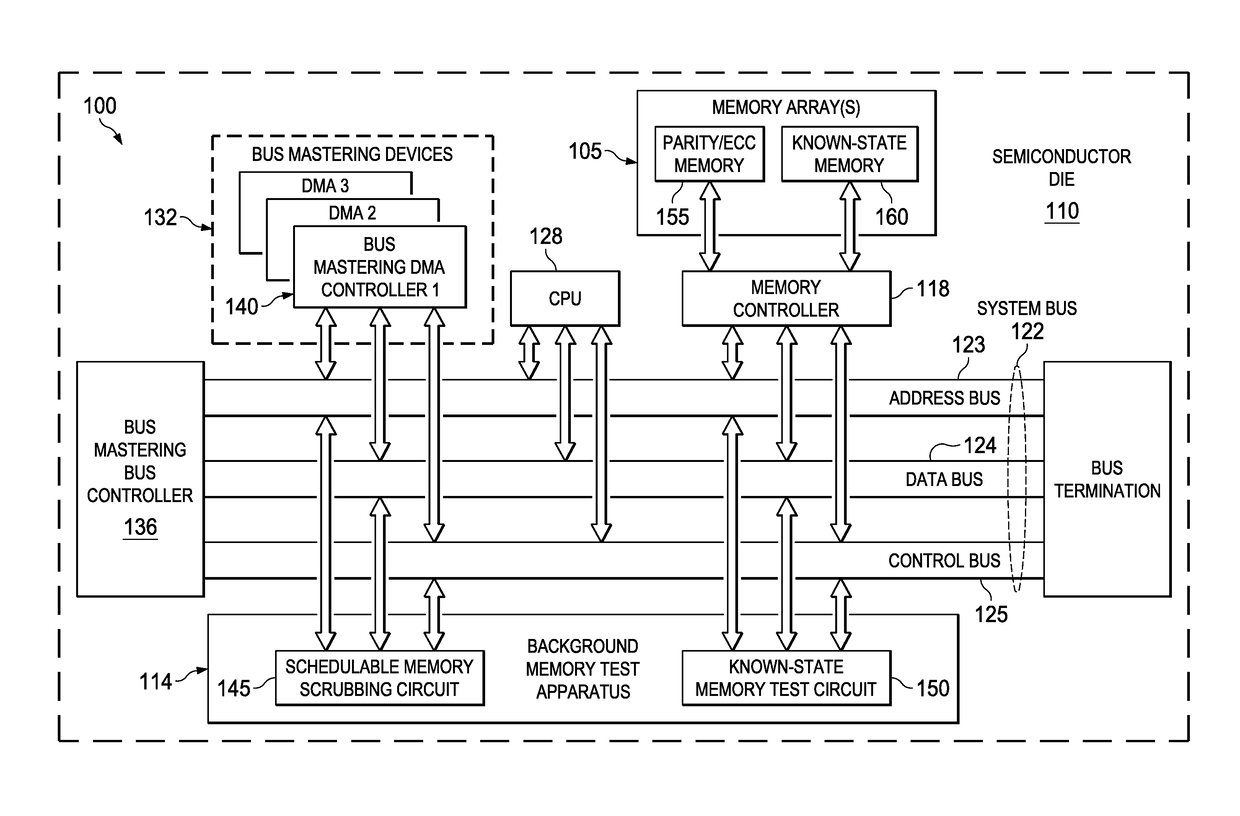
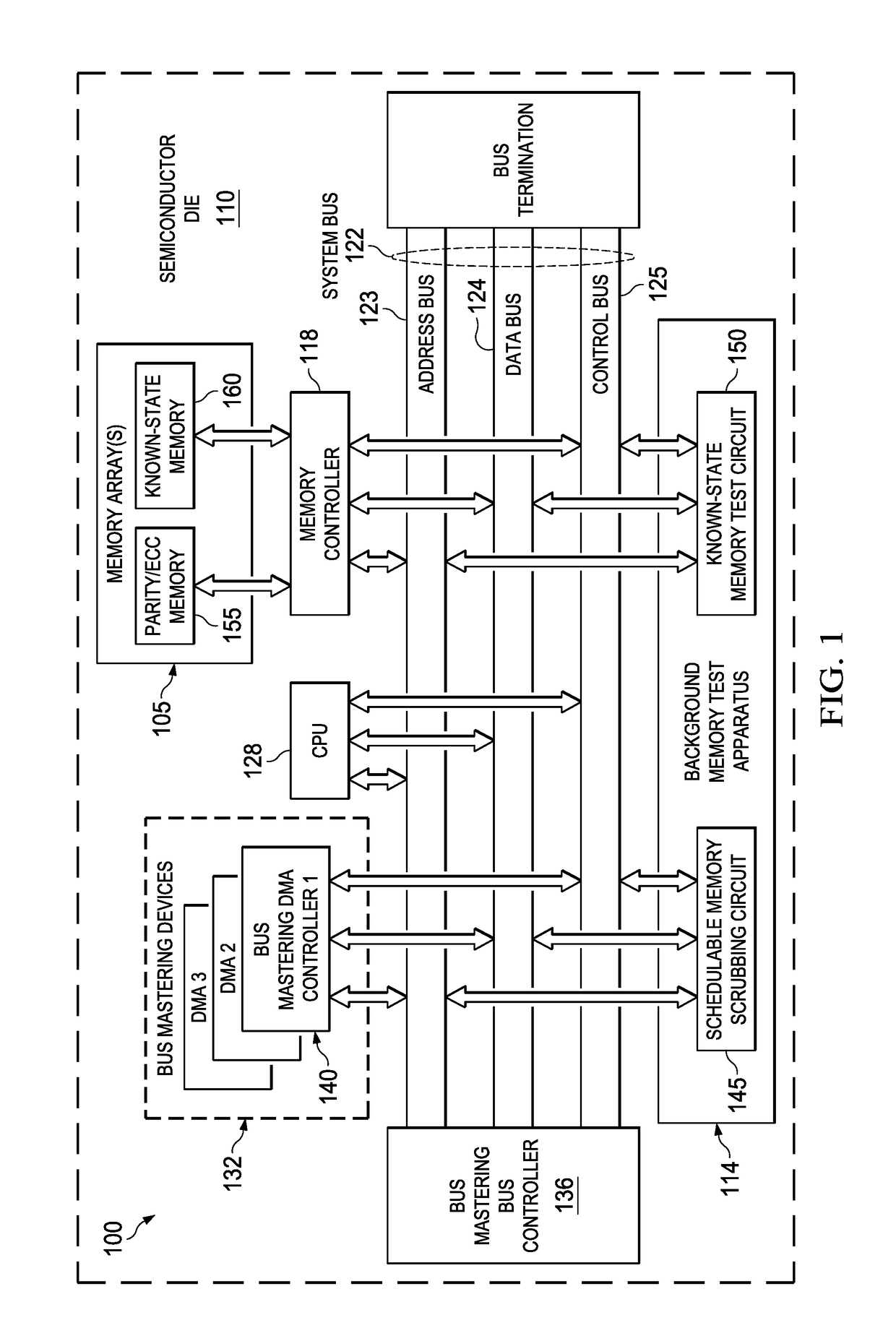
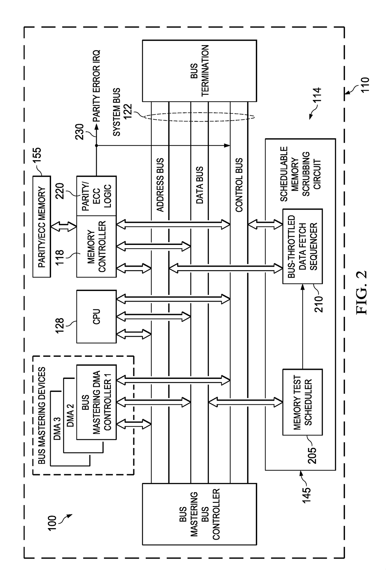
[0023]FIG. 1 is a block diagram of an integrated computing system 100 including one or more memory arrays 105 and BGMTA 114 according to various example embodiments of the invention. The memory arrays 105 and the BGMTA 114 are integrated with other components of the computing system 100 into a common semiconductor package. Various components of the integrated computing system 100 may be fabricated on one or more semiconductor die(s) 110 included in a common semiconductor package.

[0024]The integrated computing system 100 includes a BGMTA 114 fabricated on the die 110. The BGMTA 114 operates cooperatively with a memory controller 118. The BGMTA 114 and the memory controller 118 are coupled to a system bus 122 and communicate via the system bus 122. The system bus 122 may be serial or parallel as is well-known in the art. Examples embodiments herein are illustrated with a parallel bus, including an address bus portion 123, a data bus portion 124 and a control bus portion 125, without l...


PUM


Abstract

A schedulable memory scrubbing circuit and/or a known-state memory test circuit (collectively, background memory test apparatus (“BGMTA”)) are located on-chip with an integrated computing system. The BGMTA operates in parallel with a system CPU but shares a system bus with the CPU. The BGMTA sequentially reads one word at a time from a block of memory to be tested during system bus idle cycles. The schedulable memory scrubbing circuit embodiment tests on-chip parity/ECC memory arrays using memory controller-implemented parity or ECC error detection to trigger error handling interrupts. The known-state memory test circuit embodiment performs CRC calculations on known-state memory arrays as each data word is read sequentially. A final resulting CRC calculation value is compared to a known CRC value for the block, sometimes referred to as a “golden CRC.” If the two CRC values differ, a CRC error interrupt is triggered for servicing by the CPU.

Description

PRIORITY CLAIM[0001]This application claims the benefit of priority under 35 U.S.C. §119(e) to U.S. Provisional Patent Application Ser. No. 62 / 252,860 titled “RUN TIME SELF-TEST OF MEMORIES USING BACKGROUND CRC”, filed on Nov. 9, 2015 and incorporated herein by reference in its entirety.TECHNICAL FIELD[0002]Embodiments described herein relate to on-chip semiconductor memory test circuits, including structures and methods associated with testing known-state memories and / or memories with parity / CRC capability.BACKGROUND INFORMATION[0003]Among the various genera of semiconductor data storage device technologies (“semiconductor memories” or simply “memories”), known-state and error detection / correction types are known. Error detection / correction types include parity and error correction code (“ECC”) memories. Today's compact computing devices (e.g., smart phones, tablet computers, industrial automation devices, automotive subsystems and the like) typically include one or both of the afo...

Claims


Application Information

Patent Timeline
IPC IPC(8): G11C29/42G11C29/44H03M13/09G06F11/10
CPCG11C29/42G06F11/106H03M13/09G11C29/44G06F11/1068G11C29/14G11C29/16G11C29/32H03M13/093G11C2029/1208G11C2029/1806G11C2029/4002G06F11/1048
Inventor VISWANATHAN PILLAI, PRASANTHLANGADI, SAYA GOUD
Owner TEXAS INSTR INC
Why Eureka
Try Eureka