Sample holder, device and method for detaching of a first substrate

a substrate and sample technology, applied in the direction of lamination, electrical equipment, applications, etc., can solve the problem of least partial adverse effect on the properties of the interconnect layer and/or the substrate or components, and achieve the effects of increasing the debonding rate, increasing the throughput, and improving economic efficiency

Active Publication Date: 2017-05-11
THALLNER ERICH
View PDF9 Cites 16 Cited by
  • Summary
  • Abstract
  • Description
  • Claims
  • Application Information

AI Technical Summary

Benefits of technology

[0019]Another advantage of the invention includes an increased debonding rate. Two, in particular blanket-bonded substrates, can be separated from one another within a few seconds by the process of the invention. The reduction of the debonding time results in an increase of the throughput and thus in higher economic efficiency.
[0020]According to one advantageous embodiment of the invention cooling units are made as cooling agents for cooling of the substrate mount / wafer chuck for accommodating and holding the substrate / substrates. They have in particular corresponding fixing elements, in particular vacuum lines. The cooling unit / units and fixing elements is / are locally separated from one another and / or can be moved independently. In particular feed inlets and drains for a cooling agent are made able to be rerouted, preferably as hose or flexible tube construction.
[0021]Embodiments of the invention describe devices / systems and methods for cooling a substrate stack and in this way enabling careful stripping. Cooling of the substrate stack (preferably indirectly, therefore without direct contact with the interconnect layer) cools the interconnect layer, in particular the cement, preferably a bonding adhesive.
[0022]One idea of the invention includes in particular in using a material for the interconnect layer which at room temperature or slightly elevated temperature is suitable for bonding of the substrates, at lower temperature embrittles at least partially, in particular completely, and thus either loses its adhesion properties to the surfaces of the substrates or can be at least separated along its volume, so that separation of the two substrates of the substrate stack from one another can take place.
[0023]The substrate stack is comprised of at least two substrates which are / have been bonded to one another by an interconnect layer, in particular a cement. Substrate stacks with more than two substrates are also conceivable, two substrates always being joined to one another using a cement. Hereinafter for the sake of simplicity, substrate stacks with two substrates are treated. The substrate stack can be fastened on a tape which has been laminated in particular onto a frame. This embodiment is used in particular for fixing of already back-thinned substrates (product substrates).
[0024]According to the invention any interconnect layer which is suitable for bonding of two substrates and which embrittles below a critical temperature can be used.

Problems solved by technology

If the fixing is limited in time, it is temporary bonding.
All these hitherto known methods have major defects which can lead to an at least partial adverse effect on the properties of the interconnect layer and / or the substrates or components which are located thereon.

Method used


Image

  • Sample holder, device and method for detaching of a first substrate
  • Sample holder, device and method for detaching of a first substrate
  • Sample holder, device and method for detaching of a first substrate

Examples


first embodiment

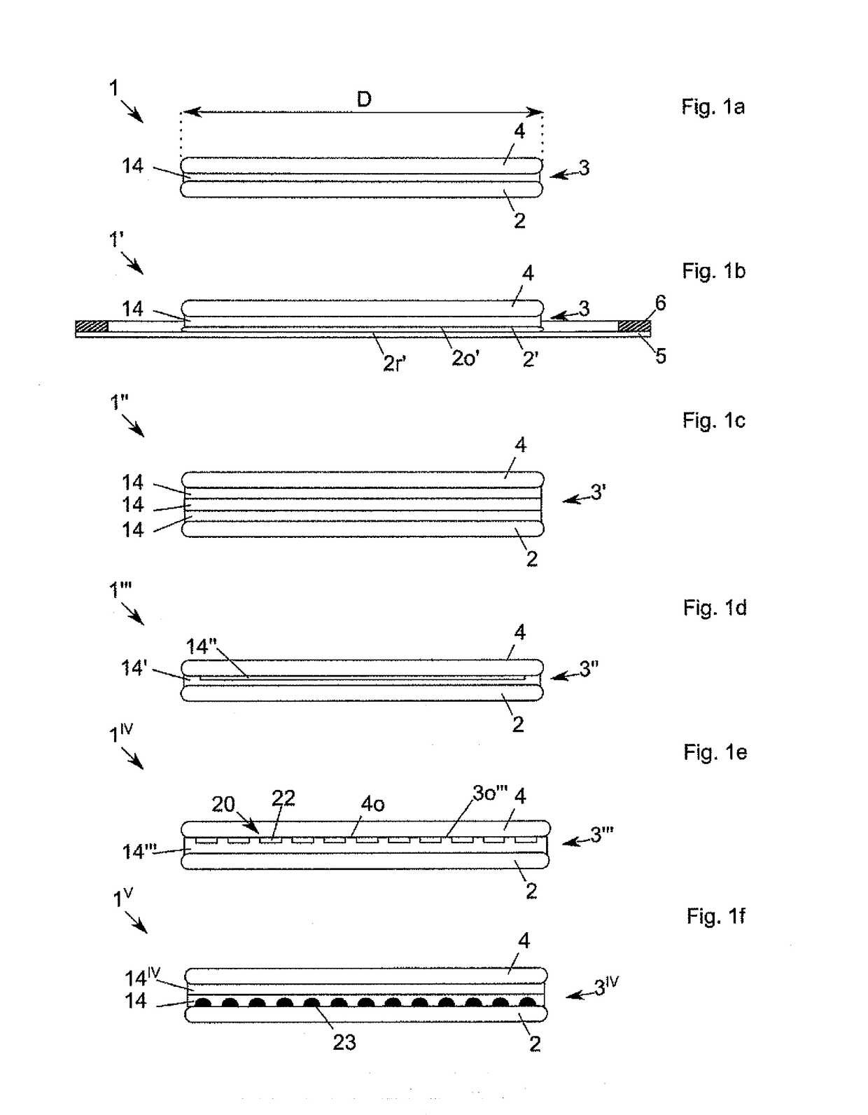
[0174]The interconnect layer 3 in the first embodiment according to FIG. 1a is comprised of a single layer which is made as a single-component system or multicomponent system.

second embodiment

[0175]In the second embodiment according to FIG. 1b the substrate stack 1′ has an in particular back-thinned product substrate 2′ which has been fixed via its surface 2o′ which has not been back-thinned by the interconnect layer 3 on the carrier substrate 4. One back-thinned side 2r′ is fixed on a film, 5, in particular a dicing tape. The film 5 is clamped on a frame 6.

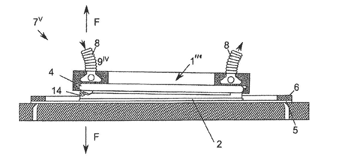
[0176]The substrate stack 1″ according to FIG. 1c is comprised of the product substrate 2 which is fixed to the carrier substrate 4 via the interconnect layer 3′ which comprises in particular several layers 14. Each of the layers 14 can be comprised of a single component or of several components. In particular not all the layers 14 need be adhesive layers.

[0177]In the embodiment according to FIG. 1d the substrate stack 1′″ is provided with an interconnect layer 3″ which is made as a ZoneBOND™ system. The interconnect layer 3″ has one adhesive layer 14″ which extends over the entire contact area between the two substra...


PUM

PropertyMeasurementUnit
temperatureaaaaaaaaaa
lengthaaaaaaaaaa

Abstract

A method and device for detaching a first substrate, which is connected to a second substrate by an interconnect layer, from the second substrate by embrittlement of the interconnect layer. A method for bonding of a first substrate to a second substrate with an interconnect layer which can be embrittled by cooling. A use of a material which can be embrittled for producing an interconnect layer between first and second substrate for forming a substrate stack. A substrate stack, formed from a first substrate, a second substrate and an interconnect layer located therebetween, the interconnect layer formed from a material which can be embrittled. A wafer chuck for holding a first substrate when the first substrate is being detached from a second substrate with fixing means which can be activated by lowering the temperature.

Description

FIELD OF THE INVENTION[0001]The invention relates to a method for detaching a substrate, a device for detaching a substrate, a method for bonding a substrate, a use of a material for producing an interconnect layer, a substrate stack formed from a pair of substrates, and an interconnect layer and a substrate mount for holding a substrate.BACKGROUND OF THE INVENTION[0002]In semiconductor technology, substrates are generally back-thinned to reduce the dimension of the components which are being formed. One of the most frequent reasons for the use of back-thinning is to produce electrically conductive interconnections through the substrate. These lines are called through silicon via (TSVs) in particular due to their frequent use in silicon substrates. Since the industrially produced substrates, in particular wafers, have a thickness of more than 500 μm, and the TSVs however only have a length of roughly 100 μm, it is necessary to remove the residual parts of the substrate. At the end o...

Claims


Application Information

Patent Timeline
Patent Type & Authority Applications(United States)
IPC IPC(8): H01L21/67B32B43/00B32B37/08H01L21/687H01L21/683
CPCH01L21/67092H01L21/67103H01L21/68714H01L21/6835B32B2457/00B32B43/006H01L2221/68318H01L2221/68381H01L2221/68327B32B37/08B32B2309/105H01L21/6836H01L2221/6834Y10S156/93Y10S156/941Y10T156/1153Y10T156/1189Y10T156/1911Y10T156/1972H01L2221/68386
Inventor THALLNER, ERICH
Owner THALLNER ERICH
Why Eureka
Try Eureka