Magnetoresistive z-axis gradient sensor chip

a gradient sensor and magnetoresistive technology, applied in the field of magnetosensing devices, can solve the problems of large size, low sensitivity of hall effect sensors, and uneven magnetic fields generated on the surface, and achieve the effects of reducing power consumption, improving sensitivity, and improving sensitivity

Active Publication Date: 2017-07-20
MULTIDIMENSION TECH CO LTD
View PDF12 Cites 8 Cited by
  • Summary
  • Abstract
  • Description
  • Claims
  • Application Information

AI Technical Summary

Benefits of technology

[0006]With respect to the existing problems above, the present invention proposes a magnetoresistive Z-axis gradiometer chip, which, in combination with a standard manufacturing process of GMR and TMR sensors and advantages of a Z-axis sensor back-bias magnet, successfully solves the shortcomings of the above problems, enabling the measurement of the gradient of the Z-axis magnetic field by using magnetoresistive sensors with in-plane sensing axes, and has several advantages relative to the Hall sensor, including smaller size, lower power consumption, and higher magnetic field sensitivity.
[0012]Preferably, when a vertical distance from the magnetoresistive sensor unit to a Y-axis center line of the corresponding flux guide device is less than or equal to ⅓*Lx, a working range of the magnetic field of the magnetoresistive sensor unit can be increased.
[0013]Preferably, the greater the vertical distance from the position of the magnetoresistive sensor unit to the Y-axis center line is, or the greater the thickness Lz of the flux guide device is, or the smaller the width Lx of the flux guide device is, the higher the magnetic field sensitivity of the magnetoresistive sensor unit is.
[0027]Preferably, the magnetoresistive Z-axis gradient sensor chip is mounted onto a PCB, the back of the PCB is provided with a permanent magnet for generating a magnetic field perpendicular to the magnetoresistive Z-axis gradient sensor chip, the PCB is placed in a casing, the casing includes a mounting bracket and a pin electrode located at the back, the PCB and the magnetoresistive Z-axis gradient sensor chip are located in the mounting bracket, and the magnetoresistive Z-axis gradient sensor chip is designed to have a saturated magnetic field higher than a magnetic field of the permanent magnet and have high magnetic field sensitivity.

Problems solved by technology

1) As InSb is not a standard material and a non-standard semiconductor manufacturing process is employed, the manufacturing process thereof is more complex with respect to the standard semiconductor manufacturing process of sensors such as TMR and GMR.
2) At present, all GMR-based and TMR-based magnetic image sensors are mainly based on the in-plane magnetic field sensing direction, and when they are applied to currency detector magnetic heads, it is necessary to use a back-bias magnet with a deep groove cut on a surface, whose shape is relatively complex. Therefore, magnetic fields generated on the surface are not evenly distributed, while a back-bias magnetic block magnetized in the Z-axis direction can be used as an InSb-based Z-axis sensor back-bias magnet, which has a relatively simple structure.
3) Compared with the GMR and TMR sensors, the Hall effect sensor has relatively low magnetic field sensitivity, poor stability (sensitivity, offset and resistance), and poor repeatability (it is difficult to control the change in the offset and the sensitivity).

Method used


Image

  • Magnetoresistive z-axis gradient sensor chip
  • Magnetoresistive z-axis gradient sensor chip
  • Magnetoresistive z-axis gradient sensor chip

Examples


first embodiment

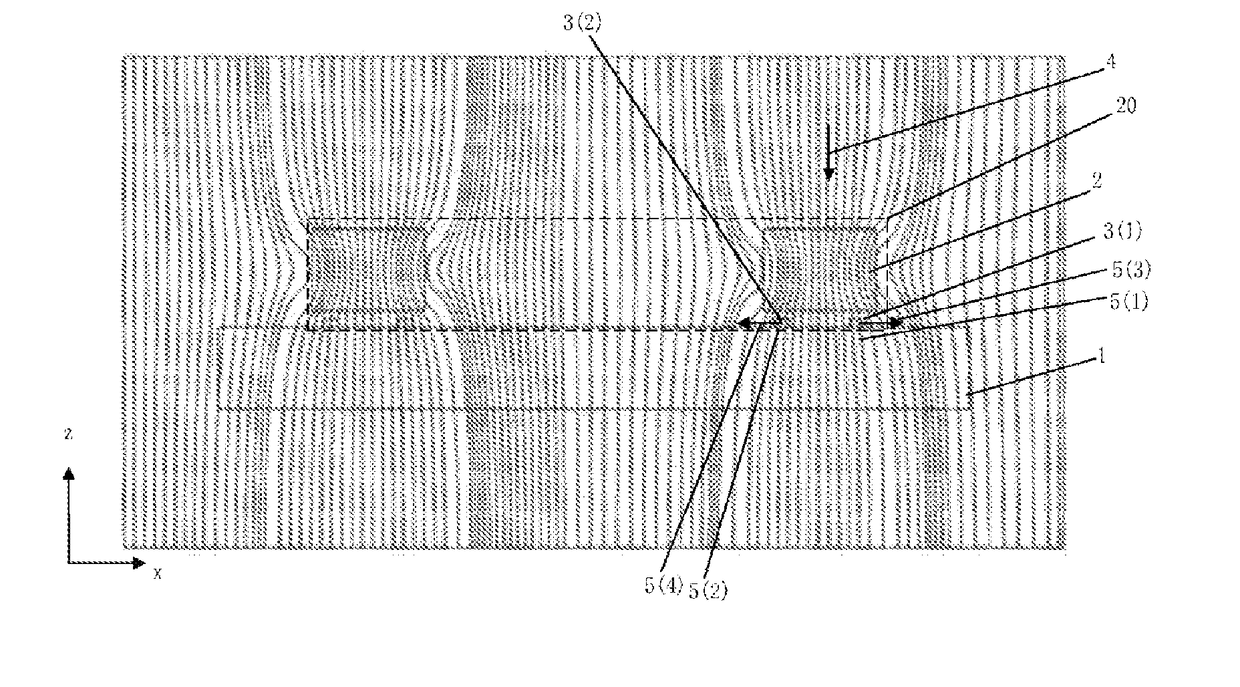
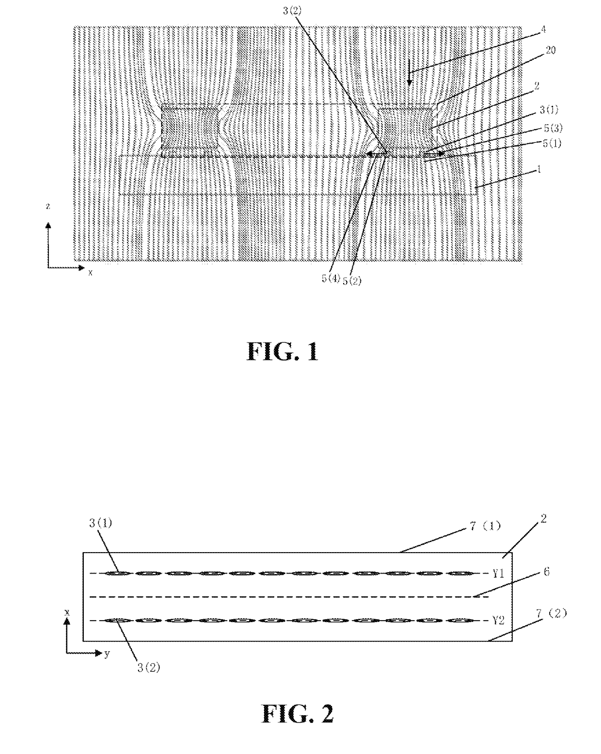
[0047]FIG. 1 is a schematic diagram of a magnetoresistive Z-axis gradiometer chip, including a Si substrate 1 and a magnetoresistive Z-axis sensor 20. The magnetoresistive Z-axis sensor 20 is located on the Si substrate 1. The magnetoresistive Z-axis sensor includes two or two groups of multiple flux guide devices 2 and magnetoresistive units 3 (which include 3(1) or 3(2) in the figure). The magnetoresistive units 3 are located above or below the flux guide devices 2. For simplification, this figure only shows the situation where the magnetoresistive units 3 are located below the flux guide devices 2, and actually the situation where the magnetoresistive units 3 are located above the flux guide devices 2 is also included. The magnetoresistive units 3 are electrically connected into a half bridge or full bridge structure gradiometer. FIG. 1 further shows the principle of measurement of a Z-axis magnetic field. After the Z-axis magnetic field 4 passes through the flux guide devices 2,...

second embodiment

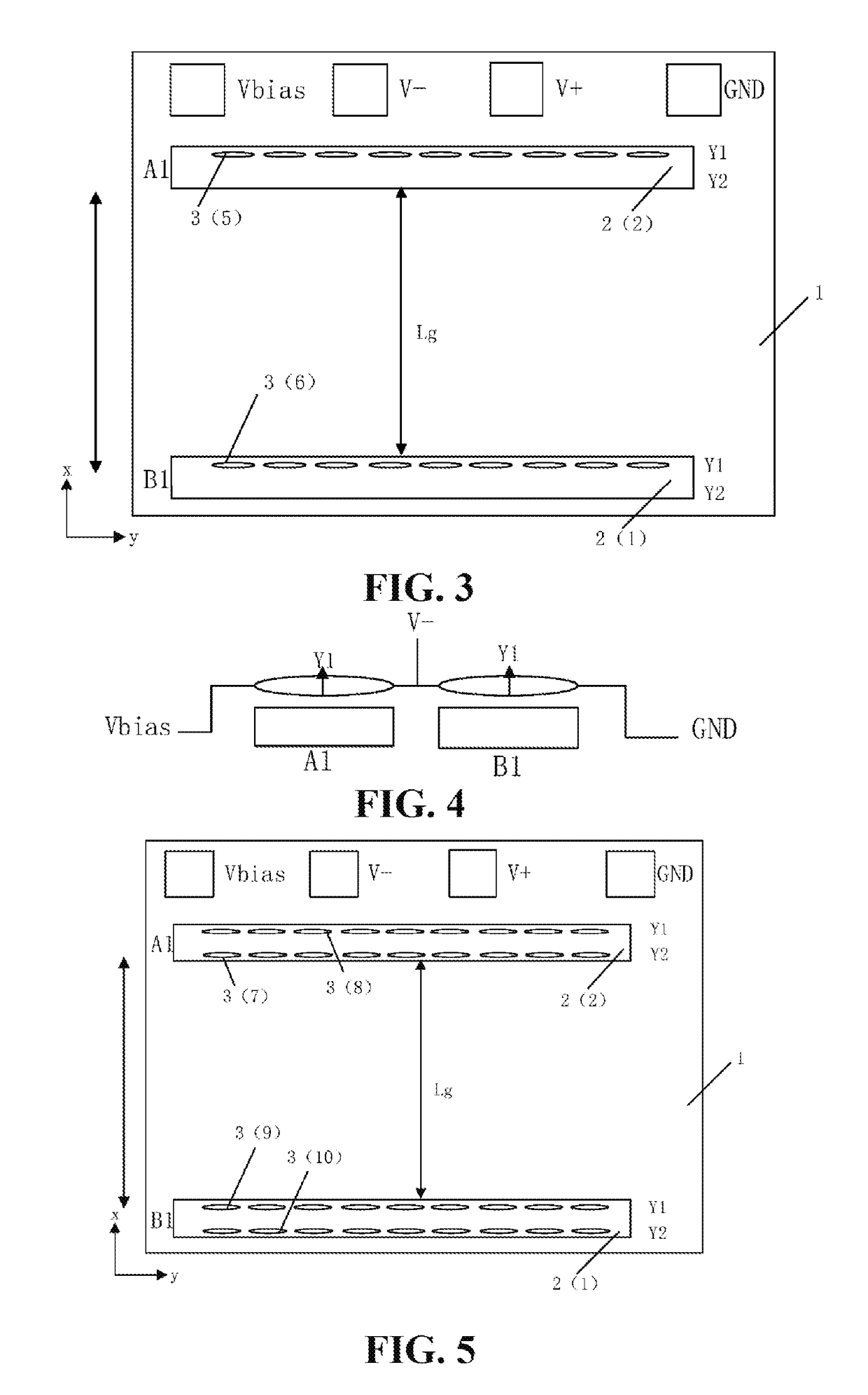
[0050]FIG. 3 and FIG. 4 are diagrams of another type of magnetoresistive Z-axis half bridge gradient sensor chip and electrical connections thereof, in which magnetoresistive units 3 (5) and 3 (6) on two bridge arms of a half bridge are located in the flux guide devices A1 and B1, respectively and occupy the same position: magnetoresistive units 3 (5) and 3 (6) are located at Y1 or Y2. For ease of description, FIG. 3 and FIG. 4 only show the situation where they are located at Y1, and they have the same magnetic field sensing direction. In this case, a half bridge output signal may be calculated in the following manner:

[0051]After a Z-axis magnetic field HZ passes through the flux guide devices, an X-axis magnetic field HX is obtained, and a correlation between HZ and HX is:

HX1=HZ1*SXZ  (1)

HX2=HZ2*SXZ   (2)

[0052]where SXZ is a magnetic field conversion parameter of the flux guide devices, which is related to the geometric structure and material property of the flux guide devices, HZ...

third embodiment

[0058]FIGS. 5-7 are a schematic structural diagram of a full-bridge-structure gradient sensor chip and diagrams of five types of electrical connections between magnetoresistive units corresponding thereto. In FIG. 5, the respective positions Y1 and Y2 corresponding to the flux guide devices A1 and B1 are occupied by magnetoresistive units 3(7)-3(10) corresponding to four bridge arms of the full bridge, respectively. In FIG. 6, two half bridges of the full bridge are corresponding to the flux guide devices A1 and B1, respectively. The magnetoresistive units at the positions Y1 and Y2 of each flux guide device have the same magnetic field sensing direction, and magnetoresistive units of two bridge arms connected to an electrode have the same magnetic field sensing direction. The output signal of the full bridge structure gradient sensor chip shown in FIG. 5 is as shown by the formulas (5)-(7), and the measured gradient of the Z-axis magnetic field is as shown by the formula (8):

V−=HX1...


PUM


Abstract

A magnetoresistive Z-axis gradient sensor chip, which is used to detect the gradient in the XY plane of a Z-axis magnetic field component generated by a magnetic medium; the sensor chip comprises a Si substrate, a collection of two or two groups of flux guide devices separated a distance Lg and an arrangement of electrically interconnected magnetoresistive sensor units. The magnetoresistive sensor units are located on the Si substrate and located above or below the edge of the flux guide devices as well; the flux guide devices convert the component of the Z-axis magnetic field into the direction parallel to the surface of the Si substrate along the sensing axis direction of the magnetoresistive sensing units. The magnetoresistive sensor units are electrically interconnected into a half bridge or a full bridge gradiometer arrangement, wherein the opposite bridge arms are separated by distance Lg. This sensor chip can be utilized with a PCB or in combination with a PCB plus back-bias magnet with casing. The sensor measures the Z-axis magnetic field gradient by using magnetoresistive sensors with in-plane sensing axes. This sensor chip has several advantages relative to a Hall Effect sensor device, including smaller size, lower power consumption, and higher magnetic field sensitivity.

Description

TECHNICAL FIELD[0001]The present invention relates to the field of magnetic sensors, and in particular, to a magneto-resistive Z-axis gradient sensor chip.BACKGROUND ART[0002]Magnetoresistive gradient sensors are widely applied to gear tooth sensing and magnetic image sensors used in as POS machine magnetic heads and currency detector magnetic heads. Under normal circumstances, magnetoresistive sensors, for example, GMR and TMR sensors, have in-plane sensing axes, whereby the magnetic field sensing direction is parallel to the surface of the chip in which the sensors are located, while a Hall Effect sensor has a Z-axis sensing direction perpendicular to the surface of the chip. At present, when used in a magnetic image sensor, a Hall Effect sensor head usually has a Hall Effect sensor made of Murata's InSb thin film material, which measures a Z-axis magnetic field component. However, both the Hall sensor that measures a Z-axis magnetic field component and a GMR or TMR sensor that me...

Claims


Application Information

Patent Timeline
Patent Type & Authority Applications(United States)
IPC IPC(8): G01R33/022G01R33/00G01R33/09
CPCG01R33/022G01R33/0011G01R33/09G01R33/093G01R33/098G01R33/0094
Inventor DEAK, JAMES GEZAZHOU, ZHIMIN
Owner MULTIDIMENSION TECH CO LTD
Why Eureka
Try Eureka