Silicon carbide semiconductor device

a technology of silicon carbide and semiconductor devices, applied in the direction of semiconductor devices, basic electric elements, electrical apparatus, etc., can solve the problems of failure of silicon carbide semiconductor devices, and achieve the effect of reducing the density of equipotential

Active Publication Date: 2017-08-03
MITSUBISHI ELECTRIC CORP
View PDF7 Cites 6 Cited by
  • Summary
  • Abstract
  • Description
  • Claims
  • Application Information

AI Technical Summary

Benefits of technology

The silicon carbide semiconductor device described in this patent reduces the risk of electrical breakdown during switching by reducing the number of equipotential lines around the outer edge of the device. This is achieved by designing the electric field strength to be weaker at the outer edge of the device, which also helps to suppress the electric field during the off-state.

Problems solved by technology

On the other hand, with regard to an SiC-SBD, there are cases where an etching residue is formed at the outer peripheral end of a Schottky electrode (a first surface electrode), which is provided on the silicon carbide semiconductor layer and the field insulation film, and there is a fear that failures of the silicon carbide semiconductor device are caused because electric field concentration occurs around an etching residue when the etching residue is formed.

Method used


Image

  • Silicon carbide semiconductor device
  • Silicon carbide semiconductor device
  • Silicon carbide semiconductor device

Examples


embodiment 1

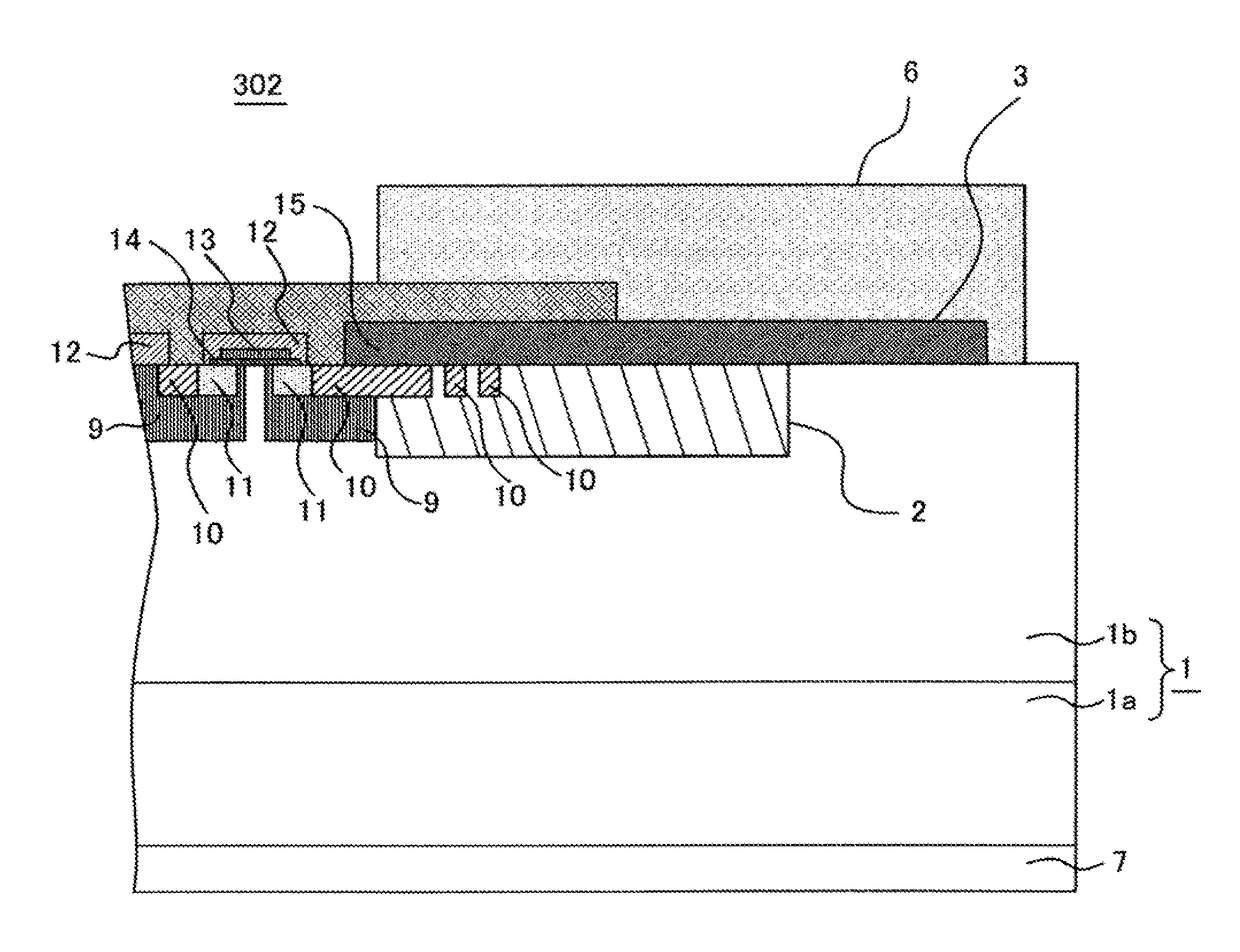
[0033]First, the configuration of a silicon carbide semiconductor device 100 in accordance with Embodiment 1 of the present invention will be described. Hereinafter, an N type SiC-SBD (Silicon Carbide Schottky Barrier Diode) in which the first conductivity-type is defined as the N type and the second conductivity-type is defined as the P type will be exemplified to be explained, but a P type silicon carbide semiconductor device in which the first conductivity-type is defined as the P type and the second conductivity-type is defined as the N type may be adopted and a PN diode or a PiN diode may be adopted instead of the SBD.

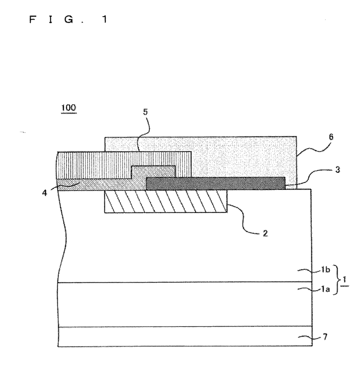
[0034]FIG. 1 is a sectional view showing the configuration of the silicon carbide semiconductor device 100 in accordance with Embodiment 1. In FIG. 1, only a cross sectional portion around the terminal end region of the silicon carbide semiconductor device 100 is illustrated, and in FIG. 1, the right side is the terminal end region side situated at the right end p...

embodiment 2

[0081]In Embodiment 1 described above, although electric field relaxation at the time of switching is attained by reducing the protruding width of the electrode pad 5, for the purpose of attaining further electric field relaxation, a high concentration terminal end well region where the P type impurity concentration is higher may be provided within a terminal end well region. On that account, as Embodiment 2, a silicon carbide semiconductor device provided with a high concentration terminal end well region will be described below.

[0082]FIG. 9 is a sectional view showing a silicon carbide semiconductor device 200 in accordance with the present embodiment. Since the silicon carbide semiconductor device 200 is different from the silicon carbide semiconductor device 100 in accordance with Embodiment 1 in the point that a high concentration terminal end well region 8 is provided thereto, hereinafter, only the high concentration terminal end well region 8 will be described, and the descri...

embodiment 3

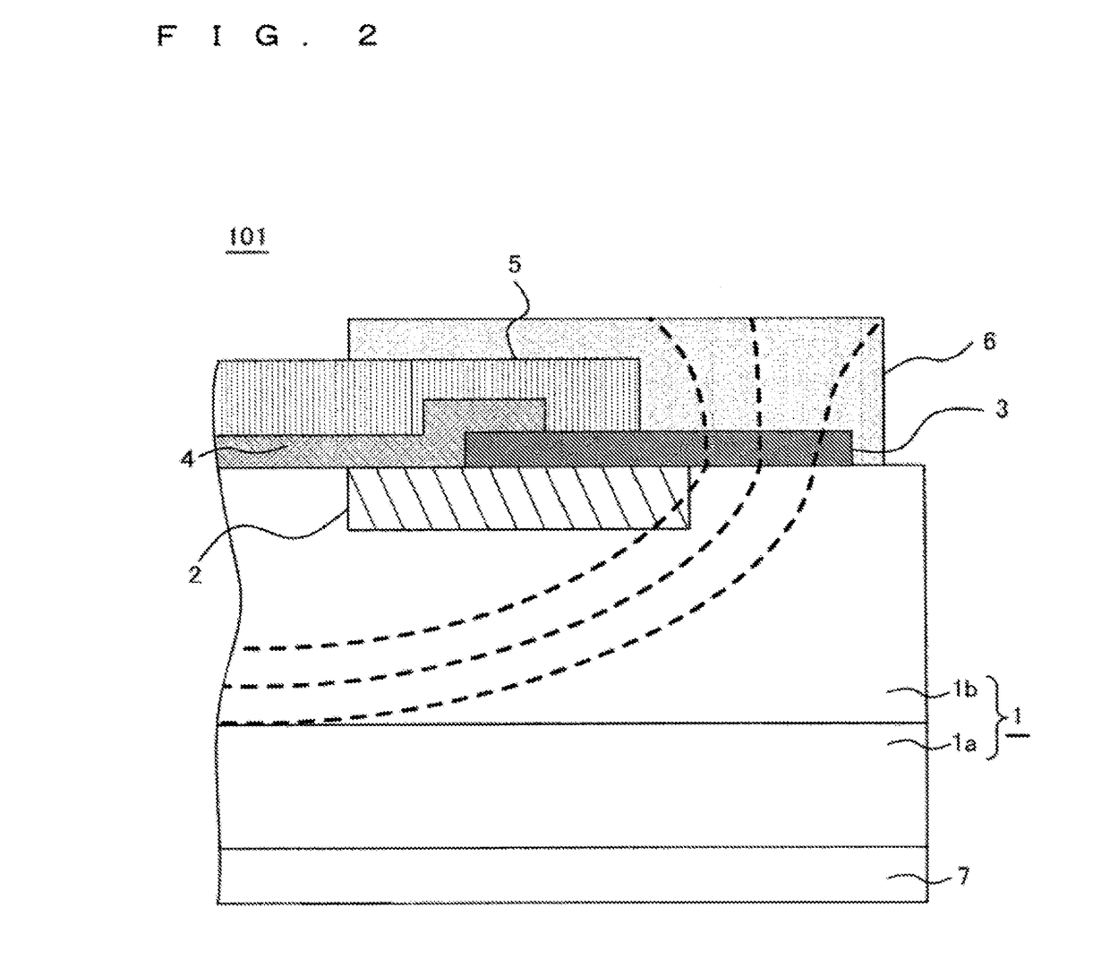
[0095]In Embodiments 1 and 2 described above, although examples of the SiC-SBD which is a diode element are described, the present invention may be applied to a switching element. On that account, as Embodiment 3, the case where the present invention is applied to an MOSFET (Metal Oxide Semiconductor Field Effect Transistor) which is a switching element will be described.

[0096]FIG. 15 and FIG. 16 are sectional views showing a silicon carbide semiconductor device 300 in accordance with the present embodiment. FIG. 15 is a sectional view of a region where a source electrode 15 described below extends up to the terminal end region side, and FIG. 16 is a sectional view of a region where a gate electrode 13 described below extends up to the terminal end region side to connect to a gate pad 16. That is, FIG. 15 is a sectional view of a region where the source electrode 15 extends to the outermost peripheral side, and FIG. 16 is a sectional view of a region where the gate electrode 13 exte...


PUM

PropertyMeasurementUnit
distanceaaaaaaaaaa
thicknessaaaaaaaaaa
distanceaaaaaaaaaa

Abstract

An object of the present invention is to provide a silicon carbide semiconductor device with which the electric field at the time of switching is relaxed and the element withstand voltage can be enhanced. The distance between the outer peripheral end of a second surface electrode and the inner peripheral end of a field insulation film is smaller than the distance between an outer peripheral end of the second surface electrode and an inner peripheral end of the field insulation film in the case where the electric field strength applied to the outer peripheral lower end of the second surface electrode is calculated so as to become equal to the smallest dielectric breakdown strength among the dielectric breakdown strength of the field insulation film and the dielectric breakdown strength of the surface protective film at the time of switching when the value of dV / dt is greater than or equal to 10 kV / μs.

Description

TECHNICAL FIELD[0001]The present invention relates to a silicon carbide semiconductor device.BACKGROUND ART[0002]In recent years, a semiconductor device prepared with silicon carbide (SiC) (hereinafter, referred to as “a silicon carbide semiconductor device”) has been attracting attention as a next-generation semiconductor device with which high withstand voltage and low loss can be realized. Since the dielectric breakdown electric field strength of SiC is about 10 times as compared with silicon (Si) which has been used for a conventional semiconductor device, in particular, the silicon carbide semiconductor device has been expected to be applied to power semiconductor devices of high withstand voltage.[0003]With regard to the silicon carbide semiconductor device, for the purpose of attaining further enhancement in withstand voltage, it has been known that, by providing a so-called terminal end region within an N type silicon carbide semiconductor layer with a P type guard ring regi...

Claims


Application Information

Patent Timeline
Patent Type & Authority Applications(United States)
IPC IPC(8): H01L29/16H01L29/78H01L29/06H01L29/66H01L29/872H01L29/36
CPCH01L29/1608H01L29/872H01L29/36H01L29/78H01L29/6606H01L29/06H01L29/0619H01L21/046H01L21/0495H01L29/0615H01L29/402H01L29/417H01L29/41741H01L29/66068H01L29/7811H01L29/7823
Inventor EBIHARA, KOHEIKOYAMA, AKIHIROKOKETSU, HIDENORINAGAE, AKEMIKAWAHARA, KOTAROWATANABE, HIROSHITAGUCHI, KENSUKEHINO, SHIRO
Owner MITSUBISHI ELECTRIC CORP
Why Eureka
Try Eureka