Antenna module and circuit module

Active Publication Date: 2017-08-10
MURATA MFG CO LTD
View PDF11 Cites 24 Cited by
  • Summary
  • Abstract
  • Description
  • Claims
  • Application Information

AI Technical Summary

Benefits of technology

[0008]A case may be assumed in which the binder resin also adheres to a region of the top surface of the multilayer module. When the binder resin adheres to the top surface of the multilayer module, the height from a to-be-mounted surface of the mounting substrate to the top of a mounting component may sometimes exceed an acceptable range. In addition, when the thickness of the multilayer module is reduced, the area of the side surface to which the binder resin adheres is decreased. Thus, the fixing strength of the multilayer module is decreased.
[0009]The present disclo

Problems solved by technology

It is difficult to control the thickness of the binder resin coating the side surface of

Method used


Image

  • Antenna module and circuit module
  • Antenna module and circuit module
  • Antenna module and circuit module

Examples


first embodiment

[0033]An antenna module according to a first embodiment of the present disclosure will now be described with reference to FIG. 1A to FIG. 4A.

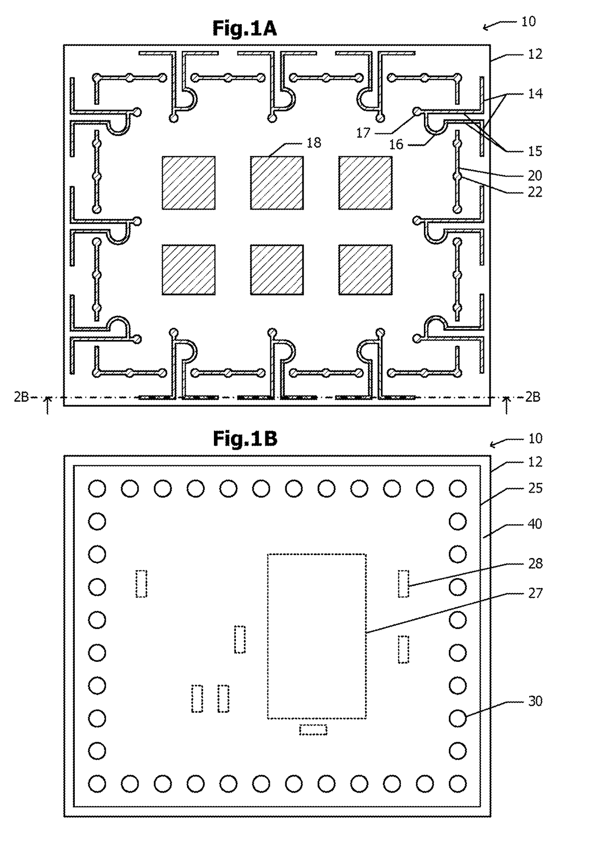
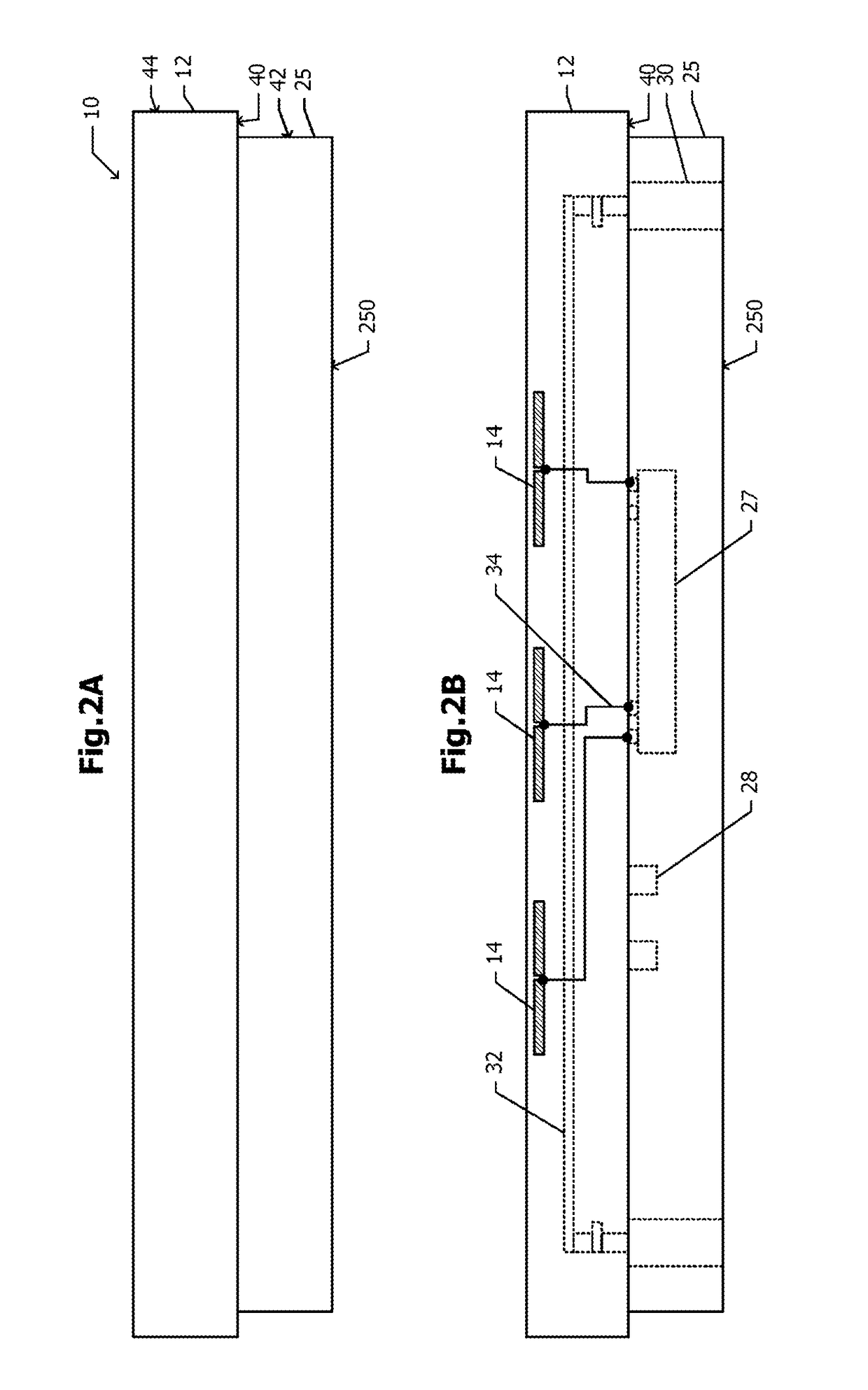
[0034]FIG. 1A is a plan sectional view of the uppermost semiconductor layer of a dielectric substrate 12 that is used in an antenna module 10. The dielectric substrate 12 has a rectangular or square planar shape. The uppermost semiconductor layer includes a plurality of printed dipole antennas 14, feeders 15, baluns (balanced-to-unbalanced transformers) 16, and a plurality of patch antennas 18. The dielectric substrate 12 is made of, for example, a ceramic, an epoxy resin, or the like. The dipole antennas 14, the feeders 15, the baluns 16, and the patch antennas 18 are each made of, for example, a conductive material such as copper. Similarly, a lower semiconductor layer is also made of a conductive material such as copper.

[0035]The plurality of dipole antennas 14 are arranged along the outer peripheral line of the dielectric substrate 12 so as...

second embodiment

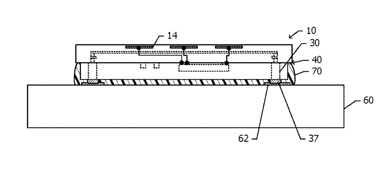
[0063]The antenna module 10 according to a second embodiment will now be described with reference to FIG. 6A and FIG. 6B. The difference between the antenna module 10 according to the second embodiment and the antenna module 10 according to the first embodiment, which is illustrated in FIG. 1 to FIG. 4, will be described below, and the description of the configuration common to the second embodiment and the first embodiment will be omitted. In the first embodiment, the antenna module 10 is mounted on the mounting substrate 60 by using the solder 36 (FIG. 4). In the second embodiment, a non-conductive paste (NCP) method is employed.

[0064]FIG. 6A is a cross-sectional view of the antenna module 10 that has not been mounted on the mounting substrate 60 and the mounting substrate 60. For example, metal bumps 37 are formed at ends of the conductor columns 30. An insulating paste 70 is applied to a mounting region of the to-be-mounted surface of the mounting substrate 60 in which the anten...

third embodiment

[0067]An antenna module according to a third embodiment will now be described with reference to FIG. 7A and FIG. 7B. The difference between the antenna module according to the third embodiment and the antenna module 10 according to the first embodiment, which is illustrated in FIG. 1 to FIG. 4, will be described below, and the description of the configuration common to the third embodiment and the first embodiment will be omitted. In the third embodiment, instead of the sealing-resin layer 25 (FIG. 2A and FIG. 2B) according to the first embodiment, a frame-shaped substrate 26 is used.

[0068]FIG. 7A is a bottom view of the antenna module 10 according to the third embodiment. FIG. 7B is a cross-sectional view taken along one-dot chain line 7B-7B of FIG. 7A. The frame-shaped substrate 26 is bonded to the bottom surface of the dielectric substrate 12. The high-frequency semiconductor device 27 and the high-frequency circuit components 28 are mounted in a region surrounded by the frame-sh...


PUM


Abstract

An antenna that is formed of a conductor pattern is disposed on a dielectric substrate. A high-frequency semiconductor device that supplies a high-frequency signal to the antenna is mounted on the bottom surface of the dielectric substrate. A plurality of conductor columns project from the bottom surface. The conductor columns are embedded in a dielectric member that is disposed on the bottom surface. An end of each of the conductor columns is exposed through the dielectric member. The dielectric member defines a mounting surface that faces a mounting substrate. A step is formed in a side surface of a composite structure that includes the dielectric substrate and the dielectric member, and a side surface extending from the mounting surface to the step is more recessed than a side surface that is located above the step.

Description

[0001]This is a continuation of International Application No. PCT / JP2015 / 079562 filed on Oct. 20, 2015 which claims priority from Japanese Patent Application No. 2014-223400 filed on Oct. 31, 2014. The contents of these applications are incorporated herein by reference in their entireties.BACKGROUNDTechnical Field[0002]The present disclosure relates to an antenna module and a circuit module that are mounted on a mounting substrate.[0003]Patent Document 1 discloses a multilayer module using a ceramic multilayer substrate. When fabricating a ceramic multilayer substrate, a ceramic green sheet that is cut into, for example, a square shape which is 100 mm long by 100 mm wide is used. Circuit components, such as a chip capacitor and a chip resistor, are mounted on the ceramic multilayer substrate. A surface conductor is formed on one surface of the ceramic multilayer substrate. The multilayer module is mounted on a mounting substrate in a position in which the surface, on which the surfa...

Claims


Application Information

Patent Timeline
IPC IPC(8): H01Q1/38H01Q21/22H01Q1/52H01L23/31H01L23/66H01L23/00H01L23/552H01L21/78H01Q23/00H01Q1/24
CPCH01Q1/38H01L2924/19104H01Q21/22H01Q1/526H01Q1/24H01L23/66H01L24/16H01L23/552H01L21/78H01L23/3121H01L23/3135H01L2223/6677H01L2223/6616H01L2224/16265H01L2924/19042H01Q23/00H01L2924/181H01L2224/16225H01L2924/0002H01L21/561H01Q19/30H01Q21/065H01Q21/067H01Q25/00H01L25/16H01L24/97H01L2924/15322H01L2924/15174H01L2924/00014H01L24/81H01L2224/97H01L2924/3025H01Q1/2283H01Q21/28H01L2924/19041H01L2924/19105H01L2924/15192H01L2924/00012H01L2224/13099H01L2224/81
Inventor YOKOYAMA, MICHIHARUAMACHI, NOBUMITSU
Owner MURATA MFG CO LTD
Why Eureka
Try Eureka