Self-Anchored Catalyst Metal-Assisted Chemical Etching

a self-anchored catalyst and chemical etching technology, which is applied in the field of wet etching, can solve the problems of affecting the performance of the device, so as to inhibit the detour or delamination of discrete metal features

Active Publication Date: 2017-08-24
THE BOARD OF TRUSTEES OF THE UNIV OF ILLINOIS
View PDF0 Cites 9 Cited by
  • Summary
  • Abstract
  • Description
  • Claims
  • Application Information

AI Technical Summary

Benefits of technology

[0006]A method of metal-assisted chemical etching comprises forming an array of discrete metal features on a surface of a semiconductor structure, where each discrete metal feature comprises a porous metal body with a plurality of pores extending therethrough and terminating at the surface of the semiconductor structure. The semiconductor structure is exposed to an etchant, and the discrete metal features sink into the semiconductor structure as metal-covered surface regions are etched. Simultaneously, uncovered surface regions are extruded through the pores to form anchoring structures for the discrete metal features. The anchoring structures inhibit detouring or delamination of the discrete metal features during etching. During continued exposure to the etchant, the anchoring structures are gradually removed, leaving an array of holes in the semiconductor structure.

Problems solved by technology

Unfortunately, current nanofabrication techniques, such as plasma etching, deep reactive ion etching and ion etching, suffer from various shortcomings, including the formation of features with rough scalloped side walls and / or surface damage and defects that degrade the device performance significantly.
A challenge with MacEtch, when the patterned metal film takes the form of discrete metal features such as metal particles or metal disks, is that uncontrolled lateral motion or delamination of the discrete metal features may occur during etching, leading to structural defects and / or non-vertical features in the etched semiconductor.

Method used


Image

  • Self-Anchored Catalyst Metal-Assisted Chemical Etching
  • Self-Anchored Catalyst Metal-Assisted Chemical Etching
  • Self-Anchored Catalyst Metal-Assisted Chemical Etching

Examples


examples

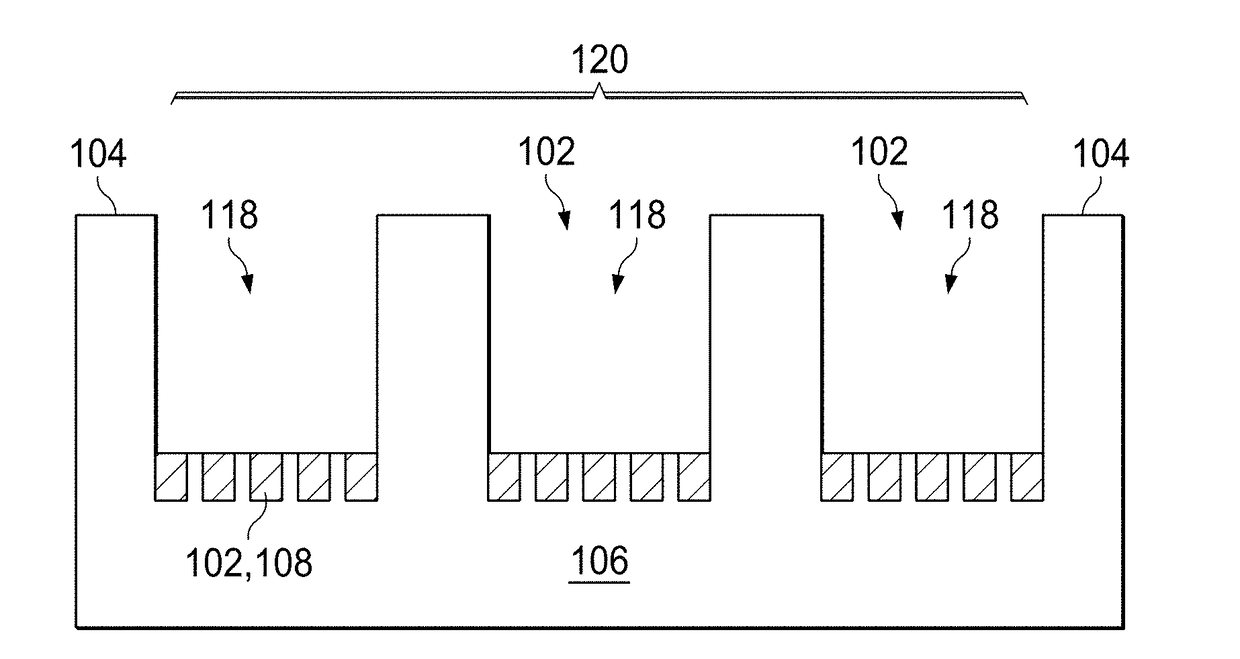
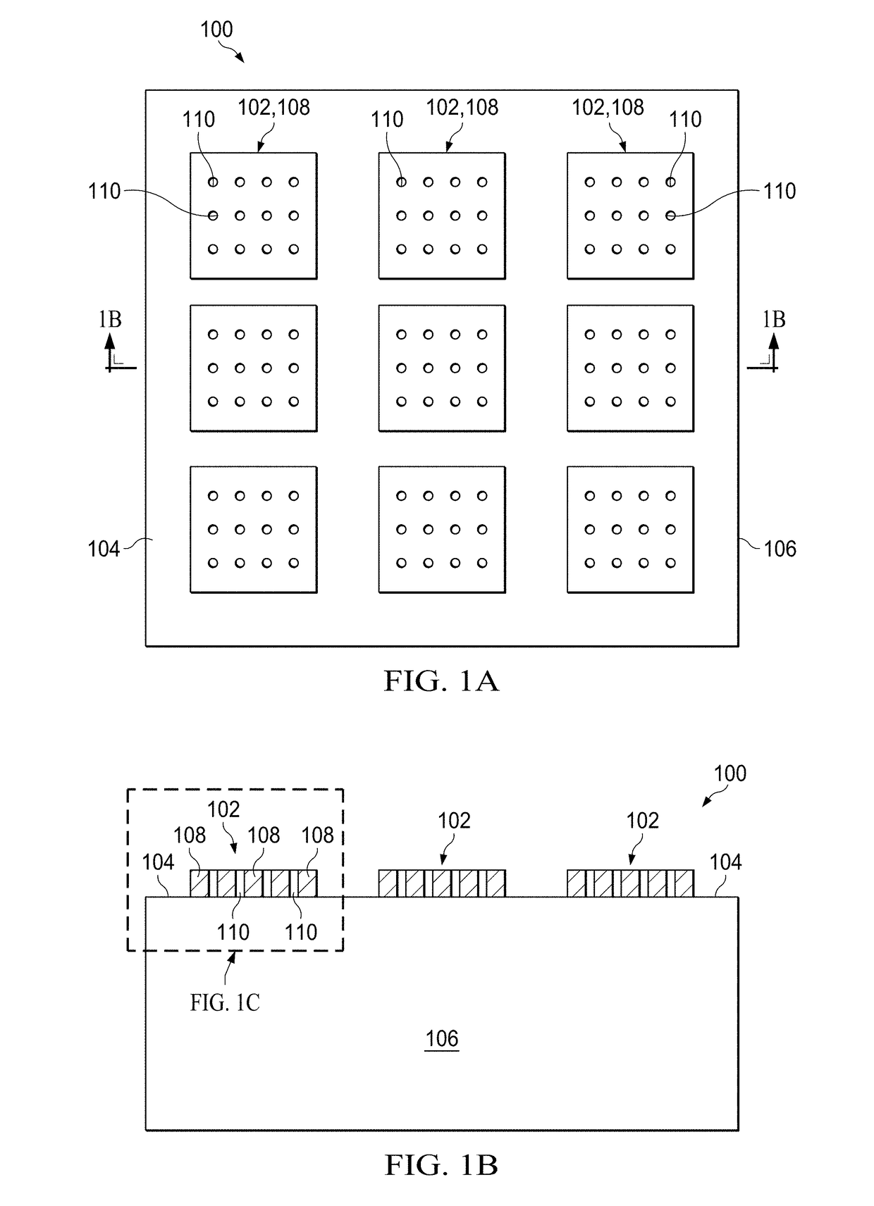
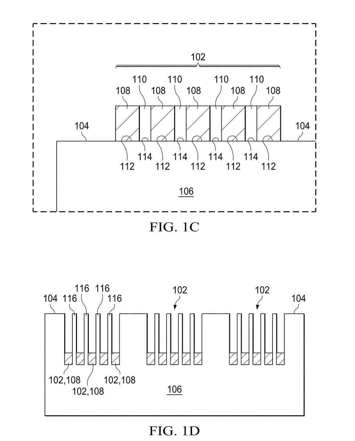
SAC-MacEtch Across Interfaces

[0038]The application of SAC-MacEtch to a semiconductor substrate including at least one interface is described in the following examples.

[0039]In the first example, the semiconductor substrate includes 2 μm-thick polysilicon over silicon oxide on boron-doped p-type (100)-oriented crystalline silicon having a resistivity of 1-50 Ω•cm, and thus the semiconductor structure includes two interfaces. The semiconductor substrate is first subjected to standard RCA cleaning processes, including organic contaminant removal in 1:1:5 ammonium hydroxide (NH4OH): hydrogen peroxide (H2O2): deionized water (DI) at 80° C., native oxide stripe in 1:10 buffer oxide etchant (BOE), and ionic contaminant removal in 1:1 hydrogen chloride (HCl): deionized water (DI).

[0040]After cleaning the semiconductor substrate, a polymer coating is deposited and lithographically patterned. The polymer coating (80 nm in thickness) is formed by spin coating 950 poly methyl methacrylate (PMMA...


PUM

PropertyMeasurementUnit
diameteraaaaaaaaaa
diameteraaaaaaaaaa
diameteraaaaaaaaaa

Abstract

A method of metal-assisted chemical etching comprises forming an array of discrete metal features on a surface of a semiconductor structure, where each discrete metal feature comprises a porous metal body with a plurality of pores extending therethrough and terminating at the surface of the semiconductor structure. The semiconductor structure is exposed to an etchant, and the discrete metal features sink into the semiconductor structure as metal-covered surface regions are etched. Simultaneously, uncovered surface regions are extruded through the pores to form anchoring structures for the discrete metal features. The anchoring structures inhibit detouring or delamination of the discrete metal features during etching. During continued exposure to the etchant, the anchoring structures are gradually removed, leaving an array of holes in the semiconductor structure.

Description

RELATED APPLICATION[0001]The present patent document claims the benefit of the filing date under 35 U.S.C. §119(e) to U.S. Provisional Patent Application Ser. No. 62 / 299,149, which was filed on Feb. 24, 2016, and is hereby incorporated by reference in its entirety.FEDERALLY SPONSORED RESEARCH[0002]This invention was made with government support under CMMI 1462946 awarded by National Science Foundation. The Government has certain rights in the invention.TECHNICAL FIELD[0003]The present disclosure is related generally to wet etching and more specifically to metal-assisted chemical etching.BACKGROUND[0004]The fabrication of semiconductor nanostructures is becoming increasingly important for both research and industrial applications. Emerging technologies and devices, such as photonic crystals, functional metamaterials and through-silicon vias (TSVs), require high resolution and high aspect ratio nanofabrication techniques for enhanced performance. Unfortunately, current nanofabrication...

Claims


Application Information

Patent Timeline
Patent Type & Authority Applications(United States)
IPC IPC(8): H01L21/306H01L21/3205H01L21/768H01L21/285H01L21/04H01L21/465H01L21/027H01L21/3213
CPCH01L21/30604H01L21/0272H01L21/32051H01L21/32139H01L21/2855H01L21/76898H01L21/28568H01L21/30612H01L21/042H01L21/0475H01L21/465H01L21/32133H01L21/0337H01L21/3086
Inventor LI, XIULINGKIM, JEONG DONGKIM, MUNHOKONG, LINGYU
Owner THE BOARD OF TRUSTEES OF THE UNIV OF ILLINOIS
Why Eureka
Try Eureka