High voltage semiconductor devices

a high-voltage semiconductor and high-voltage technology, applied in semiconductor devices, transistors, electrical appliances, etc., can solve the problems of complex structures with much smaller dimensions, exacerbate the whole problem, and increase the difficulty of forming a deeper implan

Inactive Publication Date: 2017-08-24
ANVIL SEMICON
View PDF2 Cites 13 Cited by
  • Summary
  • Abstract
  • Description
  • Claims
  • Application Information

AI Technical Summary

Benefits of technology

[0070]The forming of the lateral extension may comprise applying a two stage photo-masking to implant the lateral extension. The lateral extension may be ion-implanted using Aluminium or Bo

Problems solved by technology

However, SiC presents new challenges in this area, most importantly as mentioned above, the electric fields in SiC are very high and so this field intensification problem is much more severe.
Consequently to extrapolate the Si solution above to SiC would result in very complex structures with much smaller dimensions to the extent of not being practical using normal production equipment.
Furthermore, the material itself presents problems; since dopant diffusion is negligible in

Method used


Image

  • High voltage semiconductor devices
  • High voltage semiconductor devices
  • High voltage semiconductor devices

Examples


Embodiment Construction

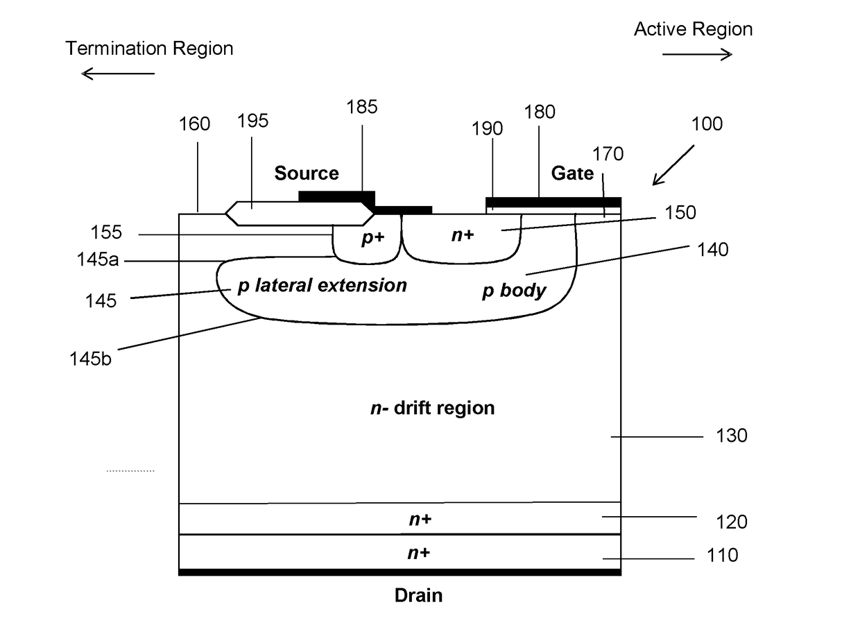
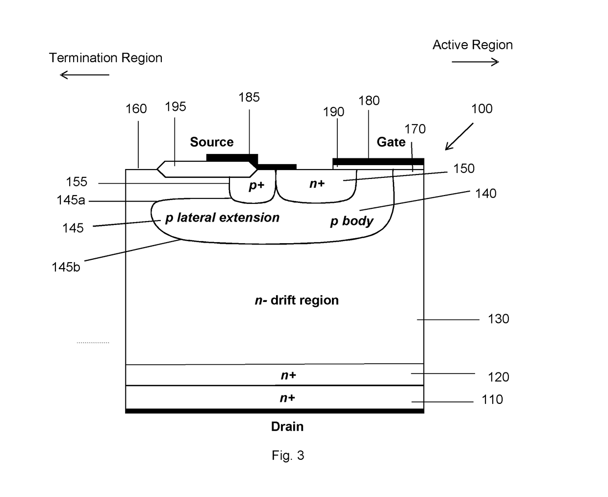
[0098]Referring to FIG. 3, an example of a SiC based vertical power semiconductor transistor 100 in the form of a metal-oxide-semiconductor field effect transistor (MOSFET) is shown. The transistor 100 is an active transistor which can be arranged as the last active transistor among an array of transistors which is located adjacent a termination region. A highly doped n-type layer (or the first semiconductor region) 120 is formed on an n-type substrate 110. A drift region 130 is formed on the first semiconductor 120. A p-type well 140 is formed within the drift region 130. An n-type highly doped source region 150 is formed within the p-type well region 140. A p-type highly doped region is formed within the p-type well 140. The highly doped p and n type regions 150, 155 are shorted using a source contact or electrode 185. A field oxide or insulator 195 is also formed adjacent the highly doped p-type region 155 and the source contact extends over the field oxide 195. The extended sour...


PUM


Abstract

We disclose a high voltage semiconductor device comprising a semiconductor substrate of a second conductivity type; a semiconductor drift region of the second conductivity type disposed over the semiconductor substrate, the semiconductor substrate region having higher doping concentration than the drift region; a semiconductor region of a first conductivity type, opposite to the second conductivity type, formed on the surface of the device and within the semiconductor drift region, the semiconductor region having higher doping concentration than the drift region; and a lateral extension of the first conductivity type extending laterally from the semiconductor region into the drift region, the lateral extension being spaced from a surface of the device.

Description

FIELD OF THE INVENTION[0001]This invention relates to a power semiconductor device, particularly but not exclusively, to a wide band-gap material based power semiconductor device.BACKGROUND TO THE INVENTION[0002]The wide band-gap of SiC (irrespective of polytype) results in a very high critical electrical field before avalanche breakdown. This critical field is roughly ten times that of Si and as a consequence one tenth of the thickness of material is needed to sustain a given voltage in the off state, which in turn leads to a much lower resistance in the on-state. This lower resistance reduces the power dissipation in the device resulting in overall system energy savings.[0003]However, care must be taken when calculating the actual breakdown voltage of a real device since the theoretical critical electric fields assume an infinite planar junction. However, in the real case field intensification occurs around the edges of a diffused region and the breakdown voltage is reduced as a s...

Claims


Application Information

Patent Timeline
IPC IPC(8): H01L29/06H01L29/08H01L21/266H01L29/20H01L29/40H01L29/10H01L29/16
CPCH01L29/0619H01L29/475H01L29/0834H01L29/1602H01L29/1608H01L29/2003H01L29/402H01L21/266H01L29/267H01L29/778H01L29/7811H01L29/7395H01L29/868H01L29/872H01L29/47H01L29/1095H01L29/8611H01L29/083H01L29/0878H01L29/0649H01L29/36H01L29/66333H01L29/7802H01L29/66674H01L29/78642H01L29/66712H01L29/7827H10B20/40
Inventor WARD, PETERLOPHITIS, NEOPHYTOSTRAJKOVIC, TANYAUDREA, FLORIN
Owner ANVIL SEMICON
Why Eureka
Try Eureka