Method for patterning quantum dot layer and method for manufacturing quantum dot color filter

a quantum dot and color filter technology, applied in the field of display technology, can solve the problems of poor resolution of quantum dot patterns formed with transfer-printing, the way of patterning the quantum dot, and the chemical environment of the quantum dot surface, so as to simplify the constituent parts, simplify the surface chemical environment and increase the light emission efficiency of the quantum dot

Inactive Publication Date: 2017-09-07
TCL CHINA STAR OPTOELECTRONICS TECH CO LTD
View PDF3 Cites 8 Cited by
  • Summary
  • Abstract
  • Description
  • Claims
  • Application Information

AI Technical Summary

Benefits of technology

[0007]An object of the present invention is to provide a method for patterning a quantum dot layer, which is capable of forming a fine quantum dot pattern; and the method helps simplify a surface chemical environment of a quantum dot to thereby increase light emission efficiency of the quantum dot.
[0008]Another object of the present invention is to provide a method for manufacturing a quantum dot color filter, which is capable of forming a fine quantum dot pattern; and the method helps simplify a surface chemical environment of a quantum dot to thereby increase light emission efficiency of the quantum dot and thus improve resolution and backlighting utilization of a display device.
[0026]The efficacy of the present invention is that the present invention provides a method for patterning a quantum dot layer and a method for manufacturing a quantum dot color filter. The method for patterning a quantum dot layer according to the present invention uses a photoresist layer having a patterned structure as a shielding layer to subject a monocolor quantum dot layer to etching to form a patterned quantum dot layer. The method simplifies the constituent components for making a quantum dot paste that is used to form a quantum dot layer and simplifying a surface chemical environment of the quantum dots to thereby increasing light emission efficiency of the quantum dot. Further, the method may manufacture a fine quantum dot pattern, greatly improving the resolution of the patterned quantum dot layer. The method for manufacturing a quantum dot color filter according to the present invention is applied to manufacturing a quantum dot color filter on the basis of the above-described method for patterning a quantum dot layer and the quantum dot color filter so manufactured has a fine quantum dot pattern, the light emission efficiency of the quantum dots being high to thereby effectively improve the resolution and backlighting utilization of a display device.

Problems solved by technology

However, such patent documents do not disclose the ways of patterning the quantum dot layers
However, in dispersing the quantum dots in the photoresist, due to various high molecule substances, such as initiation agents, monomers, polymers, and additives, involved in the photoresist, chemical environments on surfaces of the quantum dots may become complicated, leading to a great influence on the light emission efficiency of the quantum dots.
However, the quantum dot patterns formed with transfer-printing have poor resolution, where edges of the patterns are in a serrated form and the adhering power between the quantum dot layer and the base requires being further improved.
Inkjet printing is also a method for forming a patterned quantum dot layer and such a method has a severe requirement for the inkjet printing device.
There is still technical barrier to maintain stability of the drops of ink jet and the precision of printing, making it not possible for use in mass production.

Method used


Image

  • Method for patterning quantum dot layer and method for manufacturing quantum dot color filter
  • Method for patterning quantum dot layer and method for manufacturing quantum dot color filter
  • Method for patterning quantum dot layer and method for manufacturing quantum dot color filter

Examples


Embodiment Construction

[0039]To further expound the technical solution adopted in the present invention and the advantages thereof, a detailed description is given to a preferred embodiment of the present invention and the attached drawings.

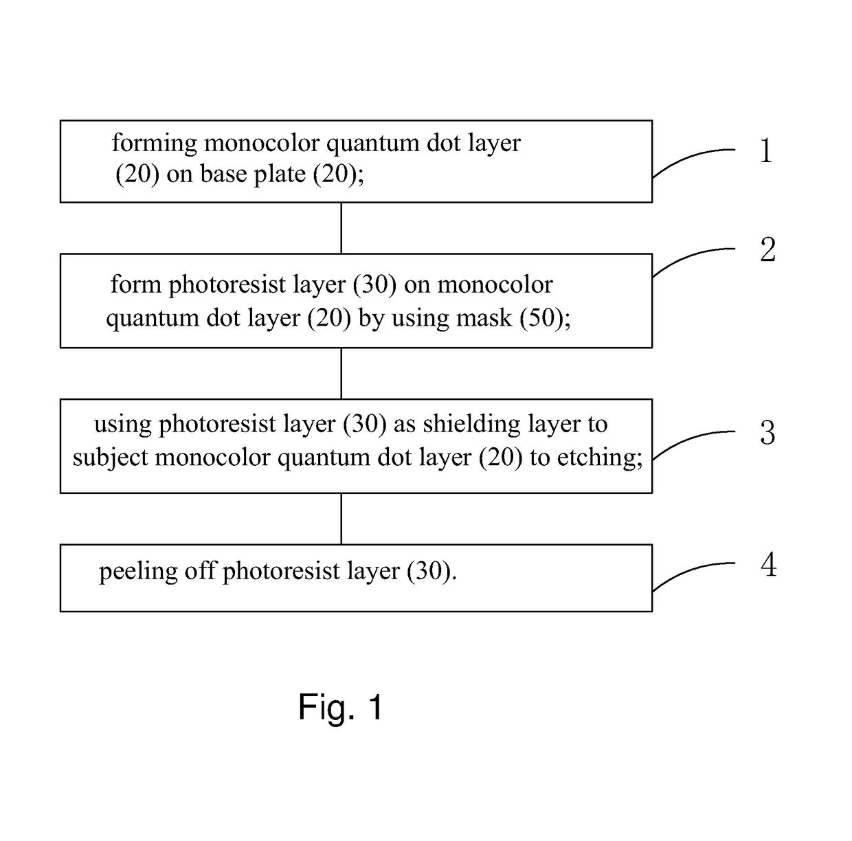
[0040]Referring to FIGS. 1-7, firstly, the present invention provides a method for patterning a quantum dot layer, which comprises the following steps:

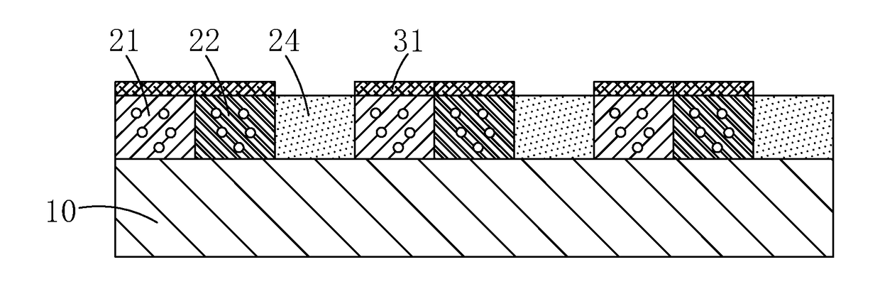
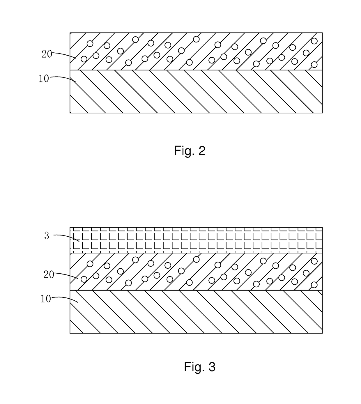
[0041]Step 1: as shown in FIG. 2, providing a base plate 10 and coating a monocolor quantum dot paste on the base plate 10 so as to obtain a monocolor quantum dot layer 20 after curing.

[0042]Specifically, the term monocolor used herein represents all kind of monochromatic colors, including red, green, and blue. The monocolor quantum dot layer 20, when excited by light, emits monochromatic light of a corresponding color, such as red light (of which the wavelength is 630-690 nm), green light (of which the wavelength is 500-560 nm), and blue light (of which the wavelength is 430-480 nm).

[0043]Specifically, the monocolor qua...


PUM

PropertyMeasurementUnit
thicknessaaaaaaaaaa
luminescence wavelengthaaaaaaaaaa

Abstract

The present invention provides a method for patterning a quantum dot layer and a method for manufacturing a quantum dot color filter. The method for patterning a quantum dot layer according to the present invention uses a photoresist layer having a patterned structure as a shielding layer to subject a monocolor quantum dot layer to etching to form a patterned quantum dot layer. The method simplifies the constituent components for making a quantum dot paste that is used to form a quantum dot layer and simplifying a surface chemical environment of the quantum dots to thereby increasing light emission efficiency of the quantum dot. Further, the method may manufacture a fine quantum dot pattern, greatly improving the resolution of the patterned quantum dot layer. The method for manufacturing a quantum dot color filter according to the present invention is applied to manufacturing a quantum dot color filter on the basis of the above-described method for patterning a quantum dot layer and the quantum dot color filter so manufactured has a fine quantum dot pattern, the light emission efficiency of the quantum dots being high to thereby effectively improve the resolution and backlighting utilization of a display device.

Description

BACKGROUND OF THE INVENTION[0001]1. Field of the Invention[0002]The present invention relates to the field of display technology, and in particular to a method for patterning a quantum dot layer and a method for manufacturing a quantum dot color filter.[0003]2. The Related Arts[0004]With the continuous development of the display technology, people increasingly demand higher and higher quality of displaying. Quantum dots (QDs) are nanometer semiconductor particles in the form of spheres or similar to spheres made of elements of II-VI groups or III-V groups, having a particle size between several nanometers and tens of nanometers. Since the particle size of QDs is less than or close to the exciton Bohr radius of the corresponding material, an quantum confinement effect is generally involved, where the energy band structure is changed from quasi-continuity of the body material to the discrete structure of the quantum dot material, making the quantum dots exhibiting unique behavior of s...

Claims


Application Information

Patent Timeline
Patent Type & Authority Applications(United States)
IPC IPC(8): G02B5/20G03F7/26G03F7/16G03F7/20G02F1/1335G03F7/00
CPCG02B5/201G02F1/133516G02F1/133617G03F7/0007B82Y20/00G03F7/20G03F7/26Y10S977/774G03F7/16H01L33/0062G02B5/206G02B5/223
Inventor LIANG, YUHENGLIU, GUOHE
Owner TCL CHINA STAR OPTOELECTRONICS TECH CO LTD
Why Eureka
Try Eureka