Printed active device

a printed active device and electronic component technology, applied in the direction of additive manufacturing processes, tubes with electrostatic control, coatings, etc., can solve the problems of reducing the production efficiency of electronic devices, and reducing the overall weight of the article. , the effect of reducing the overall weight of the articl

Active Publication Date: 2017-11-30
BRITISH TELECOMM PLC
View PDF0 Cites 3 Cited by
  • Summary
  • Abstract
  • Description
  • Claims
  • Application Information

AI Technical Summary

Benefits of technology

[0011]Thus, embodiments of the present invention provide for the production of a three dimensional article by way of the additive manufacturing process. The use of such a manufacturing process allows for the production of a three dimensional article having potentially complex internal characteristics with the integration of active electronic components such as diodes and triodes within the fabric of the article. Due to the production and integration of active electronic components as part of the article manufacturing process, there is no requirement for post-production assembly or installation of electronic components. Thus, manufacture of articles with installed electronic components can occur contemporaneous with the manufacture of the substantive three dimensional structure of the article. This relieves the manufacturing process from considerations of post-production assembly and installation of electronic components, such as burden approaches of the prior art that require multi-part manufacture with accessible integration interfaces and the like. Further, the cost of manufacture is dramatically reduced due to the use of additive manufacturing process, especially where small numbers of articles are required such as in prototyping or proof-of-concept manufacture, or in remote or inaccessible locations such as in orbit or space.
[0012]The inclusion of active electronics within the fabric of a three dimensional article will reduce the overall weight of the article due to the absence of additional components, appendages. Furthermore, articles can be made more streamlined, with electronic componentry embedded within the article, such as internally in an imperceivable, undetectable and / or unobtrusive location within the article. Where the active electronic component is embedded in the article, the component can be protected from exposure to fluids such as moisture or air. The ability of additive manufacturing to produce articles on the micro-scale provides for potentially ‘intelligent’ (in the sense of including electronic componentry) articles in all manner of applications, including: electronics embedded within cellular telephone cases or covers; electronics embedded within cable sheaths; electronics embedded within fabric or clothing; electronics embedded within cases, covers, walls or other structural elements of other devices such as consumer or entertainment devices; electronics in spare-parts; and the like.
[0014]A particular advantage of the use of thermionic electronic components is the benefits of such components over silicon equivalents such as silicon transistors. Thermionic components have considerable robustness and provide improved analogue signal transfer properties. For example, thermionic components are highly resistant to electromagnetic pulses and solar flare activity providing particular benefits on application to satellites technology or critical infrastructure systems.
[0015]While the use of thermionic electronic components has been largely superseded by semiconductor equivalents, the inventors have realised the surprising benefits of such components in the field of additive manufacturing based on the simplicity of manufacturing such components, capabilities for which now exist in the field of additive manufacturing, the effectiveness of such components and their reliability.

Problems solved by technology

Use of additive manufacturing to produce electrical or electronic devices has been severely constrained since additive manufacturing is not suitable for manufacturing complex modern electronic components from many disparate materials.
This requirement for post-manufacture assembly and / or installation has the considerable disadvantage that component locations, sockets and routes must be accessible in an additively-manufactured product.
Accordingly, the hugely beneficial characteristics of additive-manufacturing of accurately producing complex, internalised and potentially inaccessible structures are entirely lost in the electronic field.
Furthermore, the requirement for post-manufacture assembly and / or installation imposes burdens of additional manufacturing steps that considerably erode the benefits of additive manufacturing.

Method used


Image

  • Printed active device
  • Printed active device
  • Printed active device

Examples


Embodiment Construction

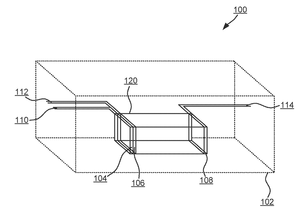
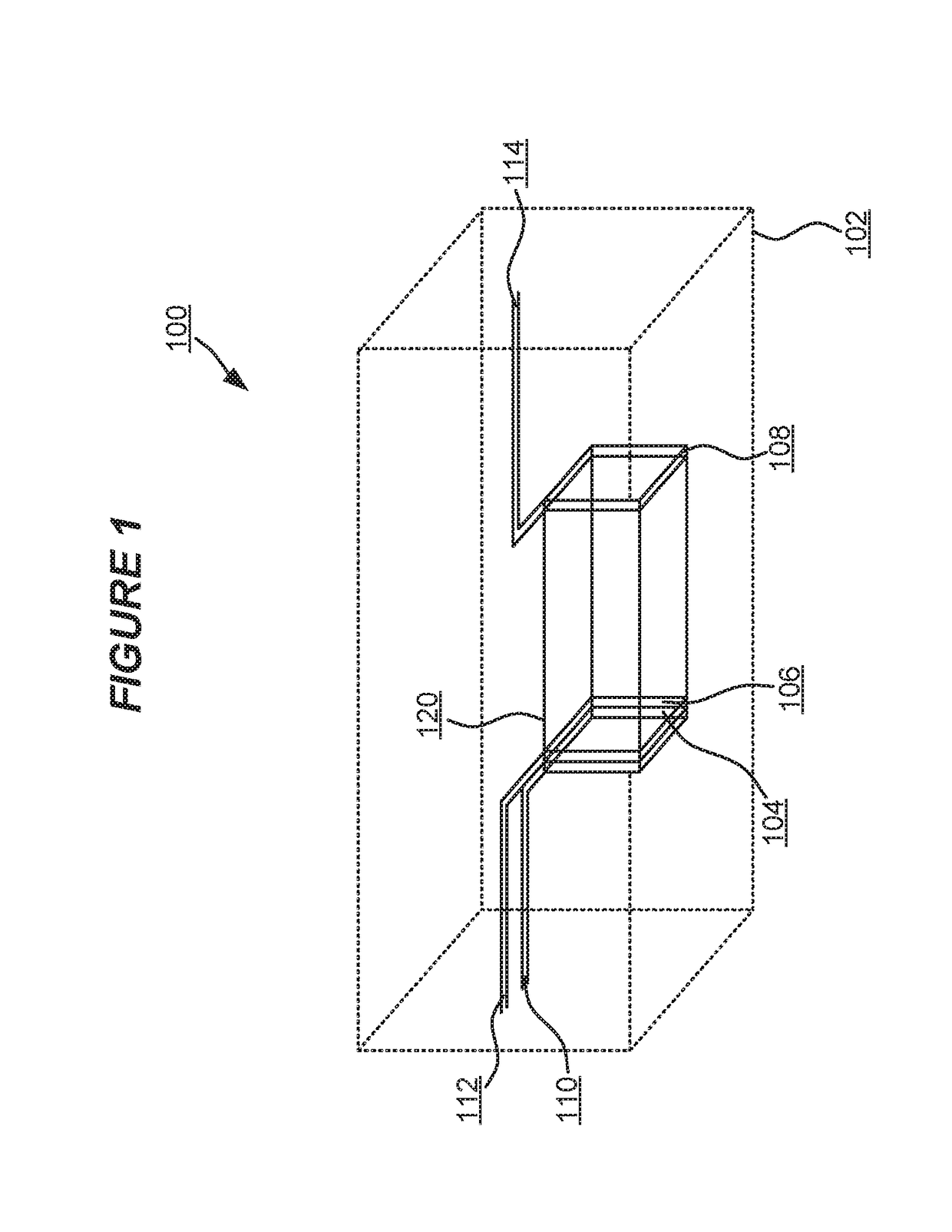
[0048]FIG. 1 depicts an exemplary three dimensional article 100 with integral diode 120 electronic component produced in accordance with embodiments of the present invention. The article 100 is constructed using an additive manufacturing approach including one or more techniques such as, inter alia: an extrusion deposition process; a material binding process such as selective laser sintering, direct metal laser sintering, selective laser melting or electron beam melting; and / or a stereolithographic approach such as photopolymerisation. Such techniques are also known as 3D printing, and a product or resulting article of such techniques is known as a 3D printed article or apparatus. The article 100 is comprised of a substantive structure 102 such as a body, framework, lattice, arrangement or other structure substantially constituting the article, otherwise referred to as the fabric of the article. For example, the article 100 can be, inter alia: a part; prototype; component; appliance...


PUM

PropertyMeasurementUnit
non-electrically conductiveaaaaaaaaaa
electrically conductiveaaaaaaaaaa
electrical potentialaaaaaaaaaa

Abstract

A method of manufacturing an article with integral active electronic component comprising: using an additive manufacturing process to: a) form a non-electrically conductive substrate; b) form a non-electrically conductive perforated layer having an aperture; c) form electrically conductive anode and cathode elements spaced in the aperture; d) deposit a conductive electrical connection to each of the elements suitable for imparting an electrical potential difference between the elements; e) form a non-electrically conductive sealing layer atop the perforated layer so as to retain and seal the aperture in the perforated layer.

Description

CROSS-REFERENCE TO RELATED APPLICATION[0001]This is a divisional of U.S. application Ser. No. 14 / 658,797, filed Mar. 16, 2015, which claims priority to EP Application No. 14 250 050.3, filed 21 Mar. 2014, the entire contents of each of which are hereby incorporated by reference.FIELD OF THE INVENTION[0002]The present invention relates to the manufacture of active electronic components. In particular it relates to the manufacture of a 3D printed article including a 3D printed 10 thermionic electronic component integral with a fabric of the article.BACKGROUND OF THE INVENTION[0003]Additive manufacturing, also known as three dimensional (3D) printing, is a process of manufacturing a three dimensional solid object from a model such as a digital model by an additive process in which material is layered, adhered, bonded or otherwise deposited successively until the solid object is formed. Such an approach is in contrast to traditional manufacturing techniques where articles are formed fro...

Claims


Application Information

Patent Timeline
Patent Type & Authority Applications(United States)
IPC IPC(8): H01J19/04H01J21/04H01J19/08B05D1/26B29C64/188H01J21/10B05D1/36B33Y10/00B33Y30/00B33Y80/00
CPCH01J21/04B29C64/188H01J21/10H01J19/08B33Y30/00B33Y80/00B05D1/265B05D1/36B33Y10/00H01J19/04B29C64/371
Inventor GHANEA-HERCOCK, ROBERT
Owner BRITISH TELECOMM PLC
Why Eureka
Try Eureka