Series and/or Parallel Connected Alpha, Beta, and Gamma Voltaic Cell Devices

a gamma voltaic and cell technology, applied in semiconductor devices, radiation electrical energy, nuclear engineering, etc., can solve the problems of reducing efficiency, affecting the operation of operators in the vicinity of the device, and consuming energy that is harmful to the operator,

Active Publication Date: 2017-12-14
CITY LABS
View PDF9 Cites 6 Cited by
  • Summary
  • Abstract
  • Description
  • Claims
  • Application Information

AI Technical Summary

Problems solved by technology

However, in the hopes of achieving reasonable power levels, the radioisotope of choice often emitted unsafe amounts of high energy radiation that would quickly degrade either semiconductor device properties within the betavoltaic battery or the surrounding electronic devices powered by the betavoltaic.
The radiated energy may also be harmful to operators in the vicinity of the device.
As a result of these disadvantages, and in an effort to gain approval from nuclear regulatory agencies for these types of devices, the choice for radioisotopes has been limited to low-energy beta (electron) emitting radioisotopes, such as nickel-63, promethium-147, or tritium.
Unfortunately, these methods embody limitations of conventional IC industry's common practices and are not conducive to the betavoltaic industry's demand for devices with increasing power production.
Unlike its solar photovoltaic counterpart, it is also beneficial to remove some of these components as their presence can reduce efficiency and degrade power performance of betavoltaic cells.
For example, typical through-vias, which extend completely through a semiconductor substrate, as described in U.S. Pat. No. 9,099,212, are deleterious to the semiconductor performance in a betavoltaic device due to reduction in active area and creation of defects in the betavoltaic semiconductor's lattice around the boundary of each via.
In addition, through-vias are costly in terms of processing equipment and time.
Vias therefore are comparatively costly in terms of the area they occupy on the cell.
In addition to occupying a larger physical space on the cell, the process of creating vias through laser ablation or plasma etching of the wafer can leave a large swath of area around the via that is unsuitable for betavoltaic use.
Furthermore, through-via reliability is traditionally low; therefore, multiple through via structures are required to improve device performance.
Similarly, other components such as conductive traces, wires, insulators, interposers, and other interconnection methods also add cost and are volumetrically and power-density inefficient for stacking betavoltaic cells.
It is also known to use surface roughness techniques to increase the area of the semiconductor and its concomitant power density of betavoltaic cells, but these techniques commonly lead to increased dark current and lowered efficiency.
These disparate elements increase the power density of betavoltaic cells and more importantly the total power of stacking arrangements; however, even with these optimizations the stacking of betavoltaic cells still requires the use of interposers, wires, solder bumps, flexible wires, wire bonds, and / or through-vias etc.
These types of interconnection of cells can be costly to produce and reduce the power density significantly.

Method used


Image

  • Series and/or Parallel Connected Alpha, Beta, and Gamma Voltaic Cell Devices
  • Series and/or Parallel Connected Alpha, Beta, and Gamma Voltaic Cell Devices
  • Series and/or Parallel Connected Alpha, Beta, and Gamma Voltaic Cell Devices

Examples


Embodiment Construction

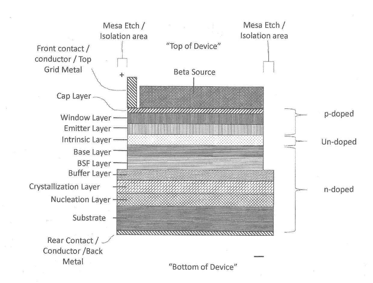
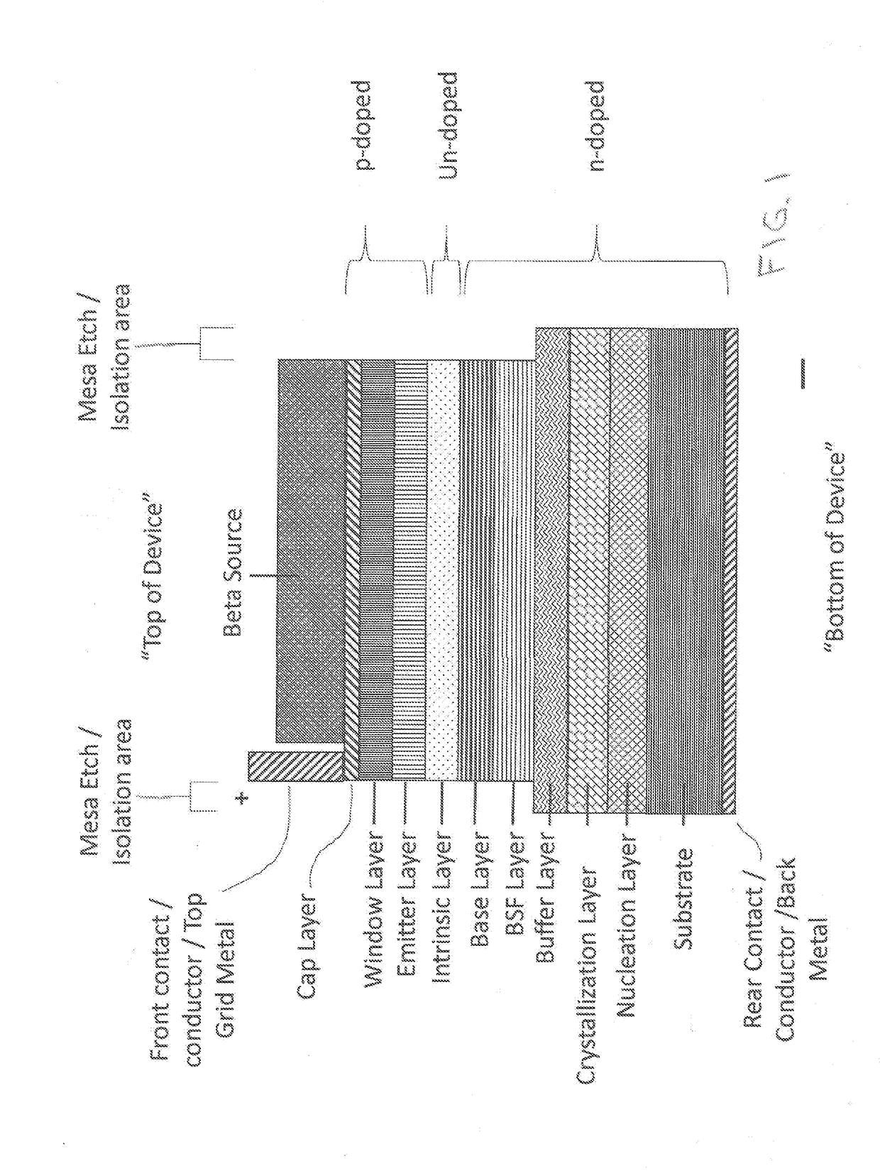
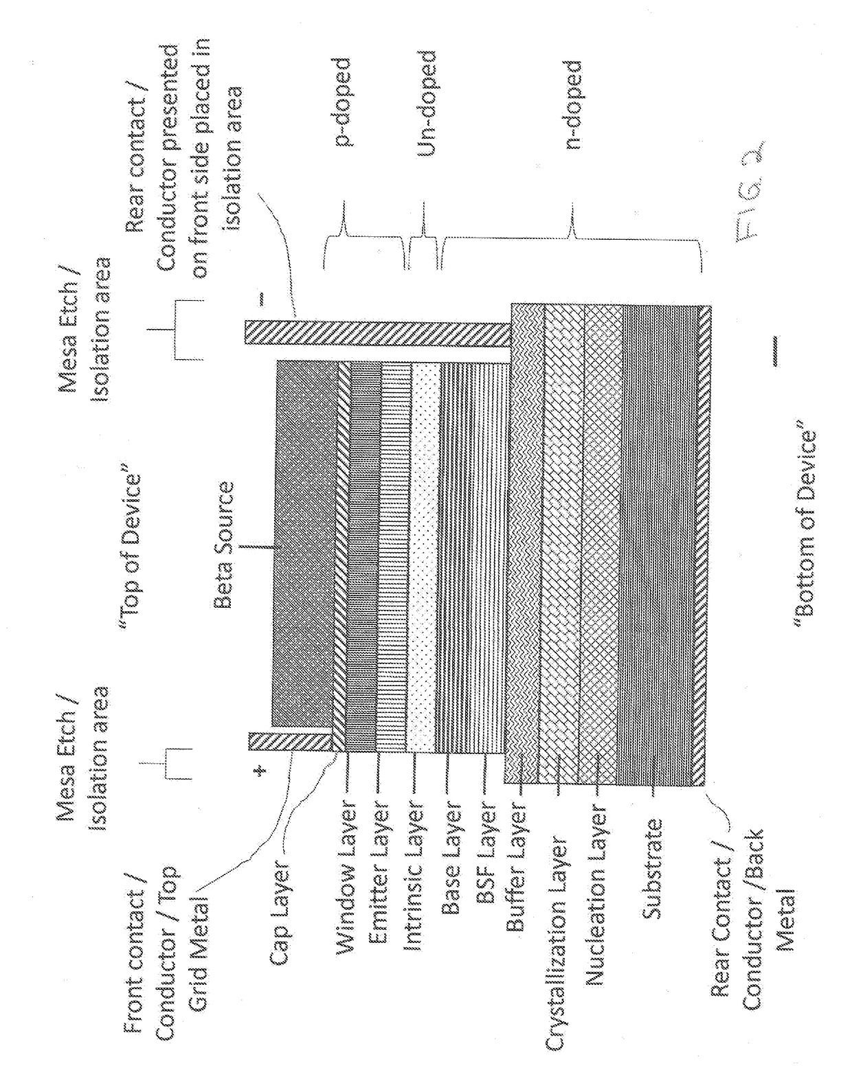
[0028]The present invention implements configurations and structures for use in creating series and / or parallel stacked betavoltaic cell devices that are both easy to manufacture, and that can be utilized across all betavoltaic junction materials (e.g. III-V materials, silicon, germanium, silicon carbide, diamond, etc.).

[0029]The push for higher power and energy density betavoltaics means that every facet of a betavoltaic system needs to be optimized. Commonly-owned U.S. Pat. No. 8,487,507 (entitled Tritium Direct Conversion Semiconductor Device) describes a method for optimizing semiconductor materials by making the substrate extremely thin or by using an epi-layer lift-off (ELO) process. This same patent describes a method for surface deposition of a thin metal tritide material directly on the surface of the semiconductor.

[0030]Solar photovoltaic cells typically have opposing polarity contacts on the top and bottom surfaces of the cell; these cells are arranged in large areal, pla...


PUM


Abstract

A device for producing electricity. The device includes a substrate having spaced apart first and second surfaces and doped a first dopant type, first semiconductor material layers disposed atop the first substrate surface and doped the first dopant type, and second semiconductor material layers disposed atop the first semiconductor material layers and doped a second dopant type. A first contact is in electrical contact with the second substrate surface or in electrical contact with one of the first semiconductor material layers. A beta particle source emits beta particles that penetrate into the semiconductor material layers; the beta particle source is proximate the uppermost layer of the second plurality of semiconductor material layers. A second contact is in electrical contact with one of the second plurality of semiconductor material layers. In one embodiment, bi-polar contacts (the first and second contacts) are co-located on each major face of the device.

Description

CROSS REFERENCE TO RELATED APPLICATIONS[0001]The present invention claims priority under 35 U.S.C. 119(e) to the provisional patent application filed on May 22, 2016 and assigned application No. 62 / 339,943. This provisional patent application is incorporated in its entirety herein.BACKGROUND OF THE INVENTION[0002]The direct conversion of radioisotope beta (electron) emissions into usable electrical power via beta emissions directly impinging on a semiconductor junction device was first proposed in the 1950's. Incident beta particles absorbed in a semiconductor create electron-hole-pairs (EHPs) that are accelerated by the built-in field to device terminals, and result in a current supplied to a load. These devices are known as Direct Conversion Semiconductor Devices, Beta Cells, Betavoltaics, Betavoltaic Devices, Betavoltaic Power Sources, Betavoltaic Batteries, Isotope Batteries etc.[0003]These direct conversion devices promise to deliver consistent long-term power for decadal time ...

Claims


Application Information

Patent Timeline
Patent Type & Authority Applications(United States)
IPC IPC(8): G21H1/06
CPCG21H1/06H01L31/03046
Inventor CABAUY, PETEROLSEN, LARRY C.ELKIND, BRET J.GRANT, JESSE
Owner CITY LABS
Why Eureka
Try Eureka