Eureka AIR delivers breakthrough ideas for toughest innovation challenges, trusted by R&D personnel around the world.

System and Method for Increasing III-Nitride Semiconductor Growth Rate and Reducing Damaging Ion Flux

a technology of iii-nitride and growth rate, applied in the field of plasma-assisted molecular beam epitaxy, can solve the problems of limiting the applicability of pambe, preventing the use of mbe for such devices, and inability to achieve high indium mole fraction layers

Active Publication Date: 2018-05-17
GEORGIA TECH RES CORP
View PDF2 Cites 3 Cited by
  • Summary
  • Abstract
  • Description
  • Claims
  • Application Information

AI Technical Summary

Benefits of technology

The patent is about a system called PAMBE that has a growth chamber, a remote plasma chamber, and a gas-conductance barrier between them. The plasma contains nitrogen and an inert gas mixture. The growth chamber has a certain pressure, while the plasma chamber has a different pressure. The gas-conductance barrier allows the pressure in the growth chamber to be lower than the pressure in the plasma chamber. The technical effect of this system is that it enables the growth of high-quality nitrogen-containing films with good adhesion and low defect rates.

Problems solved by technology

These relatively low growth rates limit the applicability of PAMBE for many device structures which require thick buffer layers to reduce defect densities resulting from heteroepitaxy.
Although the ultra clean environment of MBE can be beneficial for the thick, undoped drift regions of p-i-n rectifiers or LEDs, the slow growth rates still preclude the use of MBE for such devices.
Such layers with high indium mole fractions are impractical in MOCVD due to the low temperature requirements for growing indium bearing alloys, while high temperatures are required for cracking ammonia.
The result for most MOCVD growth of InGaN is very low growth rates and highly inefficient precursor usage.

Method used


Image

  • System and Method for Increasing III-Nitride Semiconductor Growth Rate and Reducing Damaging Ion Flux
  • System and Method for Increasing III-Nitride Semiconductor Growth Rate and Reducing Damaging Ion Flux
  • System and Method for Increasing III-Nitride Semiconductor Growth Rate and Reducing Damaging Ion Flux

Examples


examples

Substrate, Apparatus, and Growth Technique

[0055]All films, unless otherwise specified, were grown in a Riber 32 MBE system with a base pressure of approximately 8×10⁻¹¹ Torr. The substrates were single-side polished 1×1 cm sapphire, 1×1 cm GaN templates, or 2″ sapphire wafers. All substrates were sputter coated with 2 μm of tantalum on the back side for heat absorption and spreading. After cleaning in a 4:1 solution of H2SO4:H2O2, the substrates were loaded into an introductory chamber on an indium-free molybdenum block, and then outgassed at 150° C. for 20 minutes. The samples were then transferred to the growth chamber and were outgassed for an additional 10 minutes at 600° C. for the GaN template substrates or 850° C. for the sapphire substrates. Any substrate temperatures listed herein were those measured by thermocouple. For all film growths, nitrogen was supplied by a Veeco UNI-Bulb RF plasma source, with several modifications which will be described later. The gas flow and RF...


PUM

PropertyMeasurementUnit
Pressureaaaaaaaaaa
Pressureaaaaaaaaaa
Pressureaaaaaaaaaa

Abstract

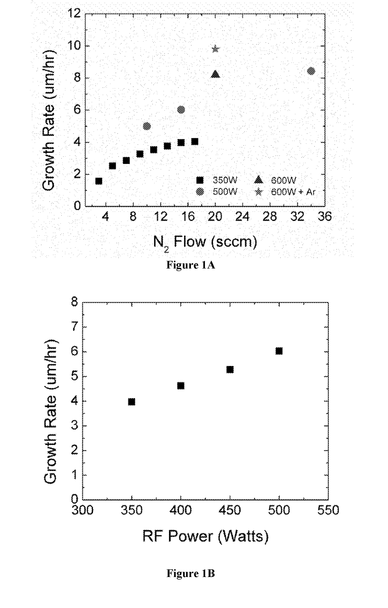
Systems and methods are disclosed for rapid growth of Group III metal nitrides using plasma assisted molecular beam epitaxy. The disclosure includes higher pressure and flow rates of nitrogen in the plasma, and the application of mixtures of nitrogen and an inert gas. Growth rates exceeding 8 μm / hour can be achieved.

Description

CROSS-REFERENCE TO RELATED APPLICATIONS[0001]This application, filed Jun. 16, 2016, claims the benefit of U.S. Provisional Patent Application Ser. No. 62 / 180,167, filed Jun. 16, 2015, entitled “Method of Increasing III-Nitride Semiconductor Growth Rate and Reduced Damaging Ion Flux Content,” the entire contents and substance of which are hereby incorporated by reference as if fully set forth below.STATEMENT OF FEDERALLY SPONSORED RESEARCH[0002]Portions of this disclosure were made with Government support under Grant Number EEC1041895. The Government may have certain rights in the disclosure.TECHNICAL FIELD[0003]The various embodiments of the disclosure relate generally to processes, methods, and systems for plasma-assisted molecular beam epitaxy (MBE). It is particularly useful for the rapid production of group III-nitride semiconductors.BACKGROUND[0004]Group III-nitride semiconductors have seen enormous commercial growth in recent years for solid state lighting and power electronic...

Claims


Application Information

Patent Timeline
IPC IPC(8): C30B23/02C30B29/40C30B31/06C23C14/22C23C14/06H01L21/02
CPCC30B23/025C30B29/406C30B31/06C23C14/221C23C14/0641H01L21/0254H01L21/02631H01L21/02576H01L21/0242C23C16/50H01L21/02458C23C16/303C23C16/452C30B23/02C23C14/0021C23C14/28C23C14/54
Inventor DOOLITTLE, WILLIAM ALANCLINTON, EVAN A.FABIEN, CHLOE A.M.GUNNING, BRENDAN PATRICKMEROLA, JOSEPH J.
Owner GEORGIA TECH RES CORP
Why Eureka
Eureka Blog
Learn More