Supercharge Your Innovation With Domain-Expert AI Agents!

Self-Latch Sense Timing in a One-Time-Programmable Memory Architecture

a one-time-programmable memory and self-latch technology, applied in static storage, digital storage, instruments, etc., can solve problems such as limiting device performance, extending the read cycle time, and data read vulnerable to nois

Active Publication Date: 2018-05-17
TEXAS INSTR INC
View PDF2 Cites 5 Cited by
  • Summary
  • Abstract
  • Description
  • Claims
  • Application Information

AI Technical Summary

Benefits of technology

This approach minimizes memory cycle time, reduces power consumption, and simplifies circuitry while maintaining accurate data sensing across varying conditions, without the inaccuracies associated with tracking circuits.

Problems solved by technology

On one hand, if the data are latched too early in the cycle, before the bit line signal has fully developed, the data read is vulnerable to error from noise.
On the other hand, latching the data later than is necessary for reliable sensing will unduly lengthen the read cycle time and thus limit the performance of the device.
It has been observed that the optimization of data path timing for read cycles in modern memory architectures can be quite difficult.
Significant device mismatch can result which, along with localized variations in device behavior of these minimum size cell transistors, necessitates additional design margin (i.e., lengthened delay between the word line drive and the sense amplifier enable signal) to be built into the timing circuit.
This additional margin adversely impacts read cycle times.
If the LATCH_DATA signal is applied to latches 6 too early in the cycle, the noise margin of the read operation is poor; if it is applied too late in the cycle, the cycle time of the memory is degraded.
It has been observed, however, that conventional tracking circuit approaches are limited in the precision with which sense amplifier or data latch timing can be attained in one-time programmable (OTP) memories.
As known in the art, the electrical behavior of OTP memory cells changes over the life of the device, for example because the charge stored at the floating gate of the bit cell transistor leaks or is otherwise weakened.
This change in behavior is typically reflected in degradation of the read performance of a programmed (i.e., “1” data state) cell over time.

Method used


Image

  • Self-Latch Sense Timing in a One-Time-Programmable Memory Architecture
  • Self-Latch Sense Timing in a One-Time-Programmable Memory Architecture
  • Self-Latch Sense Timing in a One-Time-Programmable Memory Architecture

Examples


Embodiment Construction

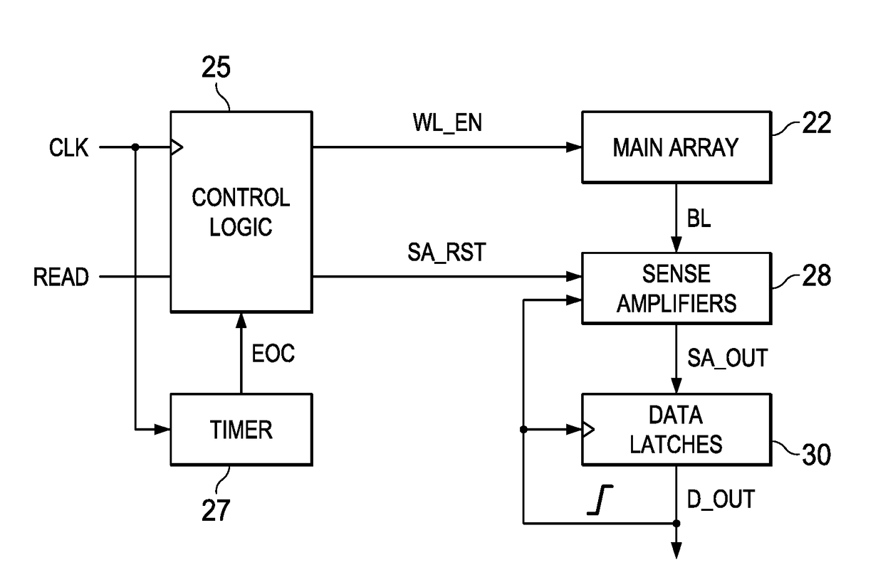
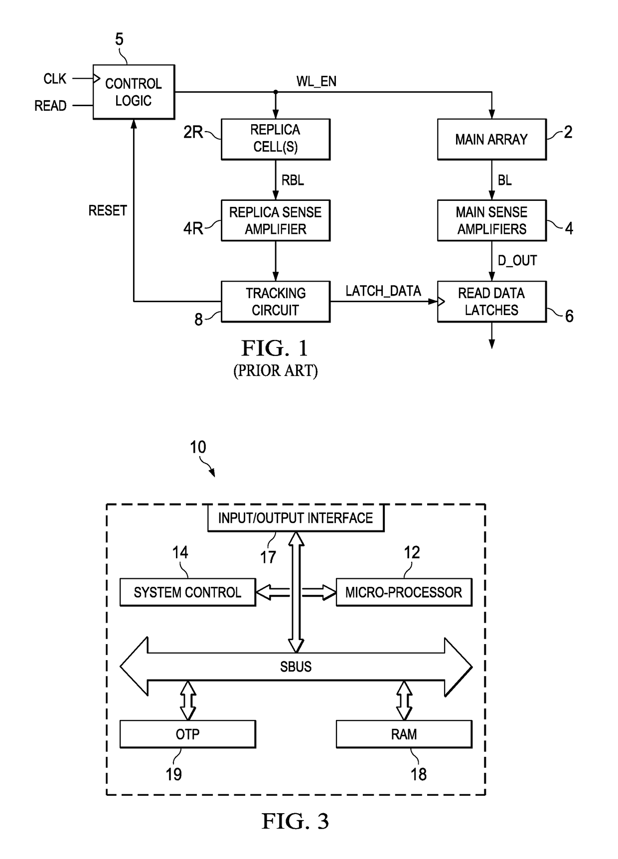
[0035]The one or more embodiments described in this specification are implemented into a one-time programmable (OTP), electrically programmable, read only memory, such as may be implemented into a microcontroller or other large scale integrated circuits, as it is contemplated that such implementation is particularly advantageous in that context. However, it is also contemplated that concepts of this invention may be beneficially applied to other applications, for example stand-alone OTP memory devices, as well as other memory technologies, particularly those for which tracking cells may not match the main memory cells in electrical characteristics and performance. Accordingly, it is to be understood that the following description is provided by way of example only, and is not intended to limit the true scope of this invention as claimed.

[0036]FIG. 3 illustrates an example of large-scale integrated circuit 10 in the form of a so-called “system-on-a-chip” (“SoC”), as now popular in ma...


PUM


Abstract

A programmable memory including a self-latching read data path. A sense amplifier senses the voltage level at a bit line, the bit line communicating the data state of a selected memory cell in its associated column. A data latch coupled to the output of the sense amplifier passes the sensed data state. Set-reset logic is provided that receives the output of the data latch in the read data path and, in response to a transition of the data state in a read cycle, latches the data latch and isolates it from the sense amplifier. The set-reset logic resets the data latch at the start of the next read cycle. In some embodiments, a timer is provided so that the latch is reset after a time-out period in a long read cycle in which no data transition occurs.

Description

CROSS-REFERENCE TO RELATED APPLICATIONS[0001]This application is a divisional of and claims priority to U.S. patent application Ser. No. 15 / 247,352, filed Aug. 25, 2016, which claims priority, under 35 U.S.C. § 119(e), of Provisional Application No. 62 / 269,737, filed Dec. 18, 2015, all of which are incorporated herein by this reference.STATEMENT REGARDING FEDERALLY SPONSORED RESEARCH OR DEVELOPMENT[0002]Not applicable.BACKGROUND OF THE INVENTION[0003]This invention is in the field of solid-state memories. Embodiments of this invention are more specifically directed to the sensing of stored data states in one-time programmable non-volatile memory.[0004]Non-volatile solid-state read / write memory devices are commonplace in many modern electronic systems, particularly in portable electronic devices and systems. Conventional types of non-volatile solid-state memory devices include those referred to as electrically programmable read-only memory (EPROM) devices. Modern EPROM memory cells i...

Claims


Application Information

Patent Timeline
Patent Type & Authority Applications(United States)
IPC IPC(8): G11C17/18G11C17/16
CPCG11C17/16G11C17/18G11C16/32G11C16/34G11C7/08G11C7/227
Inventor QIU, YUNCHENTOOPS, DAVID J.DAVIS, HAROLD L.
Owner TEXAS INSTR INC
Features
  • R&D
  • Intellectual Property
  • Life Sciences
  • Materials
  • Tech Scout
  • Unparalleled Data Quality
  • Higher Quality Content
  • 60% Fewer Hallucinations
Learn More