Flat gate commutated thyristor

a thyristor and flat gate technology, applied in the direction of semiconductor devices, basic electric elements, electrical apparatus, etc., can solve the problems of limiting the electrical and thermal contact, reducing the thermal resistance, and limiting the minimum dimension as well as the density of the cathode segment b>4, so as to improve the thermal performance, reduce the thermal resistance, and increase the contact area

Active Publication Date: 2018-07-19
HITACHI ENERGY SWITZERLAND AG
View PDF4 Cites 8 Cited by
  • Summary
  • Abstract
  • Description
  • Claims
  • Application Information

AI Technical Summary

Benefits of technology

[0022]In an exemplary embodiment, the cathode electrode has a thickness of at least 10 μm, exemplarily a thickness of at least 15 μm. The larger the distance between the level of the upper surface of the cathode metallization and the level of the upper surface of the gate metallization is, the better is the separation between a molybdenum (Mo) disc, which is used for contacting the cathode metallization layer in a standard press pack, and the gate metallization. A sufficient separation between the molybdenum disc and the gate metallization can avoid that small particles can cause a short circuit between the molybdenum disc and the gate metallization.
[0023]In an exemplary embodiment, a space between neighboring cathode electrodes is filled up with an insulating layer, and a continuous cathode conta

Problems solved by technology

Accordingly, issues related to step coverage of these layers can result.
Also, the steps in the wafer surface reduce the space available for the cathode electrodes 3, and, therefore, limit the electrical and thermal contact.
Besides the limitation of the electrical and thermal contact, the steps in the wafer surf

Method used


Image

  • Flat gate commutated thyristor
  • Flat gate commutated thyristor
  • Flat gate commutated thyristor

Examples


an embodiment

AND AN EMBODIMENT

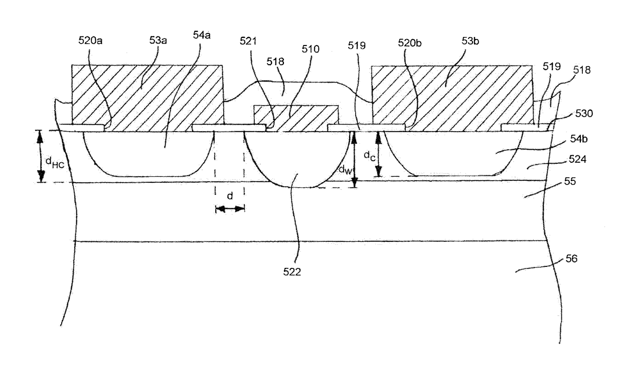
[0037]In FIGS. 5 to 7 there is shown a comparative example of a turn-off power semiconductor device. This comparative example does as such not fall under the scope of the claims. However, the comparative example serves for a better understanding of the claimed invention. FIG. 5 shows a top view onto the turn-off power semiconductor device, FIG. 6 shows a cross-section thereof along a line AA′ in FIG. 5, and FIG. 7 shows a partial cross-section, which is an enlarged portion of the cross-section shown in FIG. 6.

[0038]The turn-off power semiconductor device according to the comparative example comprises a semiconductor wafer 51, which is exemplarily a silicon wafer, having a first main side 530 and a second main side 531 opposite to the first main side 530. It comprises a plurality of gate commutated thyristor (GCT) cells 52 (which is an example for a thyristor cell in the claims) and a plurality of diode cells 512. Each GCT cell 52 comprises in the order from the firs...


PUM


Abstract

The invention relates to a turn-off power semiconductor device comprising a plurality of thyristor cells, each thyristor cell comprising a cathode region; a base layer; a drift layer; an anode layer; a gate electrode which is arranged lateral to the cathode region in contact with the base layer; a cathode electrode; and an anode electrode. Interfaces between the cathode regions and the cathode electrodes as well as interfaces between the base layers and the gate electrodes of the plurality of thyristor cells are flat and coplanar. In addition, the base layer includes a gate well region extending from its contact with the gate electrode to a depth, which is at least half of the depth of the cathode region, wherein, for any depth, the minimum doping concentration of the gate well region at this depth is 50% above a doping concentration of the base layer between the cathode region and the gate well region at this depth and at a lateral position, which has in an orthogonal projection onto a plane parallel to the first main side a distance of 2 μm from the cathode region. The base layer includes a compensated region of the second conductivity type, the compensated region being arranged directly adjacent to the first main side and between the cathode region and the gate well region, wherein the density of first conductivity type impurities relative to the net doping concentration in the compensated region is at least 0.4.

Description

FIELD OF THE INVENTION[0001]The present invention relates to a turn-off power semiconductor device according to the preamble of claim 1 and to a method for manufacturing such turn-off power semiconductor device.BACKGROUND OF THE INVENTION[0002]From DE 26 25 917 A1 there is known a semi-conductor device including a semi-conductor body with four layers of alternate P and N conducting types, these layers constitute a thyristor whose outermost layers form emitter junctions with adjacent layers. The semi-conductor body also includes an integrated field effect transistor part for bridging one of the emitter junctions of the thyristor. The source and drain of the field effect transistor include regions of the same conductivity type, one of which forms the emitter layer adjacent to the bridged emitter junction and the other of which comprises a region ohmically connected to the layer adjacent to the emitter layer and of the same type of conductivity as the emitter layer. The field effect tr...

Claims


Application Information

Patent Timeline
IPC IPC(8): H01L29/10H01L29/745H01L29/06H01L29/08H01L29/417H01L29/66
CPCH01L29/1066H01L29/745H01L29/0696H01L29/0839H01L29/102H01L29/41716H01L29/66363H01L29/36H01L29/66393H01L29/744H01L29/0692
Inventor ARNOLD, MARTINVEMULAPATI, UMAMAHESWARA
Owner HITACHI ENERGY SWITZERLAND AG
Why Eureka
Try Eureka