

Inexpensive, Earth-Abundant, Tunable Hole Transport Material For CdTe Solar Cells
a technology of earth-abundant tunable hole and solar cell, which is applied in the direction of organic semiconductor devices, solid-state devices, semiconductor devices, etc., can solve the problems of manufacturing or durability concerns, severe device performance degradation,
- Summary
- Abstract
- Description
- Claims
- Application Information
AI Technical Summary
Benefits of technology
Problems solved by technology
Method used
Image

Examples
example i
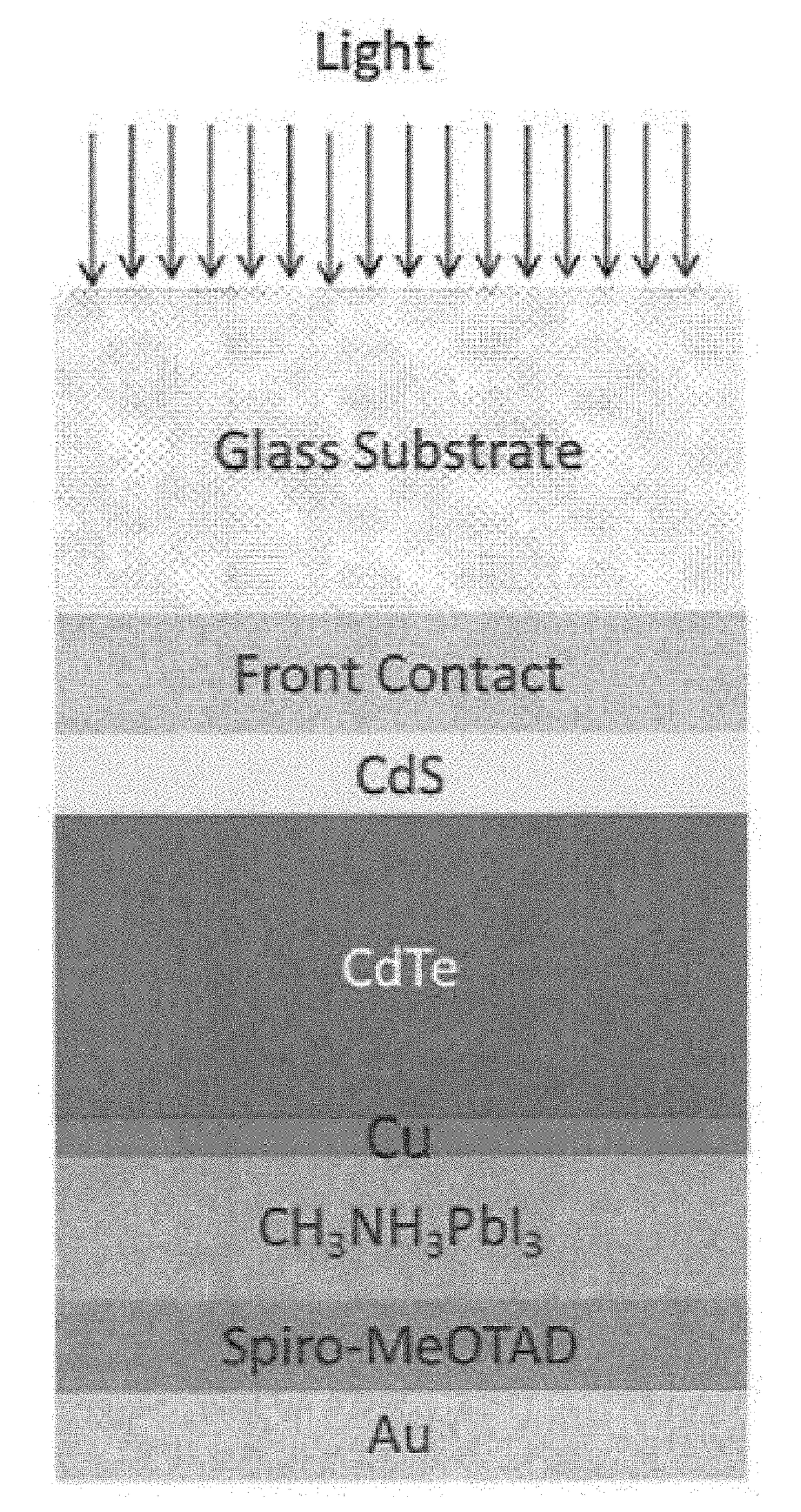
[0078]This Example describes the application of methylammonium lead halide perovskite (CH3NH3PbBryI3−y, MAPbBryI3−y) films as hole transport layers in CdTe thin film solar cells.
[0079]Experimental Methods
[0080]Window, cadmium sulfide (CdS), and absorber, cadmium telluride (CdTe), layers were deposited by a vapor assisted transfer mechanism. The device structure of CdS / CdTe solar cells used in this Example is depicted in FIG. 3A, where CdS / CdTe layers were grown on a front electrode coated on a sodalime glass substrate. About 3 nm Cu was deposited onto CdCl2-treated CdTe and annealed in dry air at 150° C. for 40 minutes. A thin layer of perovskite (PK) MAPbX3 (X═Cl, Br, I) of thickness—300 nm was then deposited onto CdTe using a spin coating. Finally, the device was completed by depositing 45 nm Au on top of MAPbX3. For the standard Cu / Au back contact deposition, similar thicknesses of Cu and Au were sequentially deposited onto the CdCl2-treated CdTe layer, and Cu diffusion was final...
example ii
[0090]A tellurium-rich surface on a CdTe layer is often employed to lower the back barrier effect and increasing the VOC and FF in the devices. In the process of the application of perovskite thin films on the CdTe surface, it was determined that a halide perovskite precursor solution, such as the non-toxic methylammonium lead iodide (MAI), can be used as an efficient surface treatment material for a CdTe surface for the formation of Te-rich surface. In this Example, the non-toxic methylammonium iodide (MAI) is shown to efficiently treat the CdTe surface. The J-V characteristics analysis indicates a reduction in the Shottky barrier at the back contact due to the surface treatment and selective removal of Cd by complexation. As a result, devices constructed with the MAI-treated CdTe absorbers exhibited higher photovoltaic parameters of open circuit voltage (VOC) and fill factor (FF) relative to similar devices prepared without organo halide treatment. The treatment time of 40 s showe...
example iii
[0107]CdTe samples were treated as described above in Example II, only with FAI instead of MAI. The samples were FAI-treated and then annealed for 5 minutes at 150° C. in an ambient environment. FIG. 13A shows the current-density Vs voltage (J-V), and FIG. 13B shows Table 4, displaying the performance characteristics, of the FAI-treated and annealed CdTe samples. FIG. 14 shows SEM images of the FAI-treated and annealed CdTe samples. FIG. 15 shows a Raman spectrum of an FAI-treated and annealed CdTe sample. As seen from FIGS. 13-15, FAI successfully treated the CdTe to create a Te-rich surface, similar to MAI.
PUM
 Abstract
Description
Claims
Application Information