
Radiation hard silicon detectors for x-ray imaging

a detector and x-ray imaging technology, applied in the field of x-ray imaging detector systems, can solve the problems of silicon detector radiation damage types, silicon detector performance degradation, and possible damage, so as to improve charge collection and maintain geometrical efficiency.

Active Publication Date: 2018-11-08
PRISMATIC SENSORS
View PDF5 Cites 5 Cited by
  • Summary
  • Abstract
  • Description
  • Claims
  • Application Information

AI Technical Summary

Benefits of technology

The present disclosure provides a detector system with improved x-ray sensitivity and robustness. The detector modules have a protective insulating layer that is resistant to damage from direct X-ray radiation. The detector system is also insensitive to misalignment, which ensures efficient and accurate detection. The technology prevents artifacts from direct illumination on the backsides or shadowing effects. The proposed technology designs enable improved charge collection.

Problems solved by technology

The main challenge with silicon is its low atomic number and low density which means it has to be made very thick for higher energies to be an efficient absorber.
The low atomic number also means the fraction of Compton scattered x-ray photons in the detector will dominate over the Photo absorbed photons which will create problem with the scattered photons since they may induce signals in other pixels in the detector which will be equivalent to noise in those pixels.
Performance degradation from radiation-induced damages is a problem for any semi-conductor detectors.
In both cases damage to silicon detector is possible.
There are two types of radiation damages in silicon detectors, bulk damage and surface damage.
The bulk damage due to the non-ionizing energy loss of incident particles is hard to happen for energy less than around 300 keV, whereas the surface damage causes most of the problems for silicon detectors used in the energy range of x-ray imaging from 40 keV to 250 keV.
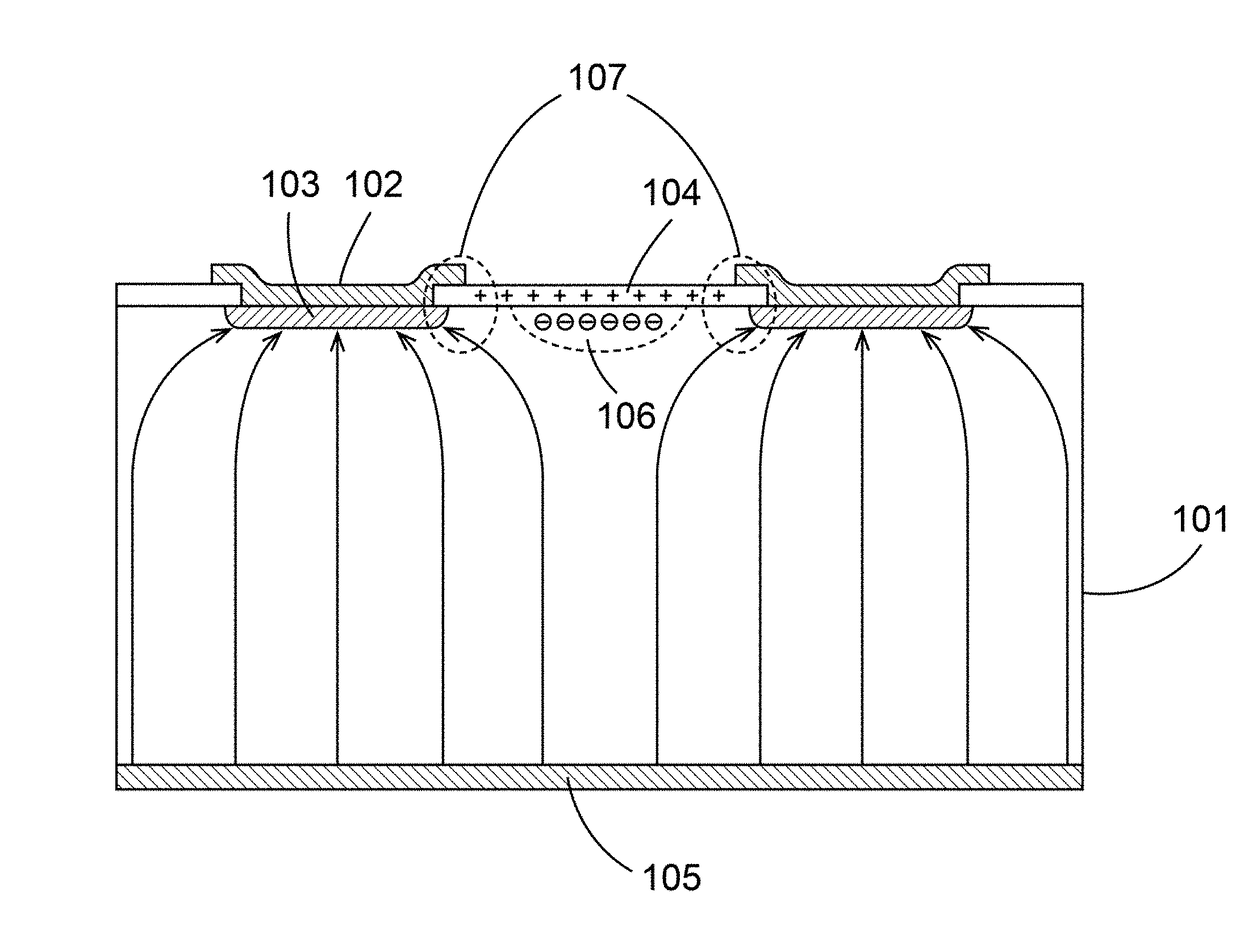
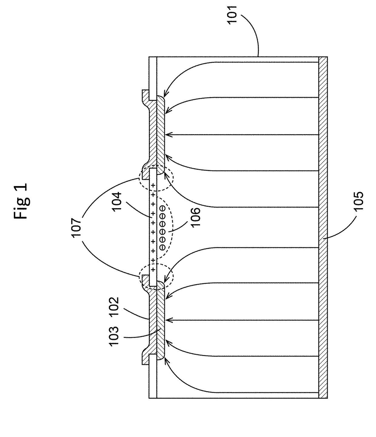
The surface damage is mainly introduced by the ionizing energy loss of charged particles or x-ray photons, which leads to the build-up of positive charges and traps in silicon dioxide and at the interface between silicon and silicon dioxide.
The deep level defects in silicon dioxide can trap holes and form fixed and positive oxide charges, which would cause some problems of the detector.
The defects induced by radiation impact electrical properties and mainly cause the following performance degradation of silicon detectors: increase of leakage current, increase of depletion voltage, increase of capacitance, formation of electron accumulation layer, decrease of breakdown voltage and charge loss near the interface between silicon and silicon dioxide.

Method used


Image

  • Radiation hard silicon detectors for x-ray imaging
  • Radiation hard silicon detectors for x-ray imaging
  • Radiation hard silicon detectors for x-ray imaging

Examples


Embodiment Construction

[0021]FIG. 8 is a schematic diagram of an x-ray detector system according to an exemplary embodiment. In this example there is shown a schematic view of an X-ray detector with x-ray source B emitting x-rays C. The detector comprises a number of detector modules stacked side by side. The detector modules comprises an edge D pointing back towards the source, and they are preferably arranged in a slightly curved overall configuration. Two possible scanning motions (E, F) of the detector are indicated. In each scanning motion the source may be stationary or moving, in the scanning motion indicated by E the x-ray source and detector may be rotated around an object positioned in between. In the scanning motion indicated with F the detector and the source may be translated relative to the object, or the object may be moving. Also in scan motion E the object may be translated during the rotation, so called spiral scanning. By way of example, for CT implementations, the x-ray source and dete...


PUM


Abstract

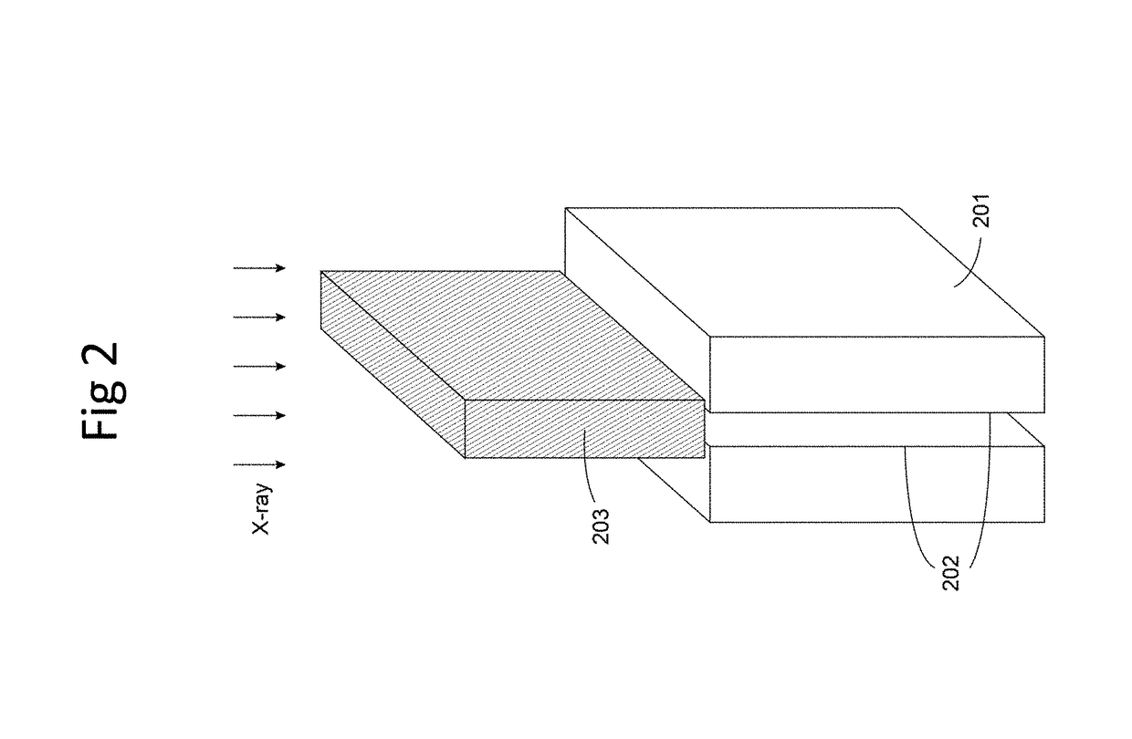
Disclosed is a detector system for x-ray imaging. The detector system includes a detector having a plurality of edge-on detector modules. Each of the edge-on detector modules includes a first edge that is adapted to be oriented towards an x-ray source and a front-side running essentially parallel to the direction of incoming x-rays. The front-side includes at least one charge collecting electrode. At least a subset of the plurality of edge-on detector modules being pairwise arranged, front-side to front-side, whereby a front-side to front-side gap is defined between the front-sides of the pairwise arranged edge-on detector modules. The pairwise arranged edge-on detector modules are associated with an anti-scatter collimator arranged in the x-ray path between the x-ray source and the edge-on detector modules and overlapping the front-side to front-side gap.

Description

TECHNICAL FIELD[0001]The present invention relates generally to a detector system for x-ray imaging and more particular to a detector system provided with edge-on detector modules.TECHNICAL BACKGROUND[0002]Among the semi-conductor material that may be used a detector materials silicon has many advantages such as high purity and low energy required for creation of charge carriers and also high mobility of charge carriers, all of which makes silicon predominating in the available semiconductor materials used primarily for radiation detectors. By implanting heavily doped layers as electrical contacts on top of low doping silicon and by applying a reverse bias to the junction to make the detector fully depleted, the radiation created charge carriers electron-hole pairs can be collected by the corresponding charge collecting electrodes.[0003]There has been a considerable interest in silicon as the material for photon-counting detectors in particular for medical imaging. By far most detec...

Claims


Application Information

Patent Timeline
Patent Type & Authority Applications(United States)
IPC IPC(8): G01T1/24G21K1/02
CPCG21K1/02G01T1/241G01T1/24G01T1/00
Inventor DANIELSSON, MATSKARLSSON, STAFFANXU, CHENGSJOLIN, MARTIN
Owner PRISMATIC SENSORS
Learn More