Transparent OLED display and manufacturing method thereof

a technology of transparent oled and manufacturing method, which is applied in the field of display techniques, can solve the problems of damage to the organic light-emitting layer f oled, low yield rate, and long film forming time, so as to achieve high yield rate, avoid damage to the light-emitting layer, and improve the effect of yield ra

Active Publication Date: 2018-11-22
WUHAN CHINA STAR OPTOELECTRONICS TECH CO LTD
View PDF0 Cites 7 Cited by
  • Summary
  • Abstract
  • Description
  • Claims
  • Application Information

AI Technical Summary

Benefits of technology

[0019]Compared to the known techniques, the present invention provides the following advantages. The present invention provides a manufacturing method of transparent OLED display, by preparing the cathode and the anode on two different substrates to effectively avoid the destruction of the light-emitting layer made of the organic light-emitting material caused by sputtering the anode at the top of OLED to improve yield rate. The use of the transparent conductive metal oxide to manufacture the cathode and the anode of the OLED display provides an effective solution to the manufacturing of transparent OLED display which requires high conductivity and high transparency for the electrode material. In addition, the two substrates can be manufactured the same time and then pressed to attach to achieve high manufacturing efficiency. The OLED display provided by the present invention is easy to manufacture and provides good performance.

Problems solved by technology

The sputtering process may damage the organic light-emitting layer f OLED when a too-high power is applied, and suffers a too-long film forming time and low yield rate when a too-low power is applied.

Method used


Image

  • Transparent OLED display and manufacturing method thereof
  • Transparent OLED display and manufacturing method thereof
  • Transparent OLED display and manufacturing method thereof

Examples


Embodiment Construction

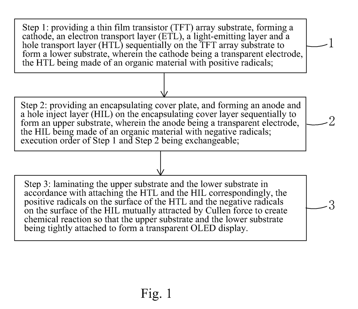
[0025]Referring to FIG. 1, the present invention provides a manufacturing method transparent OLED display, which comprises the following steps:

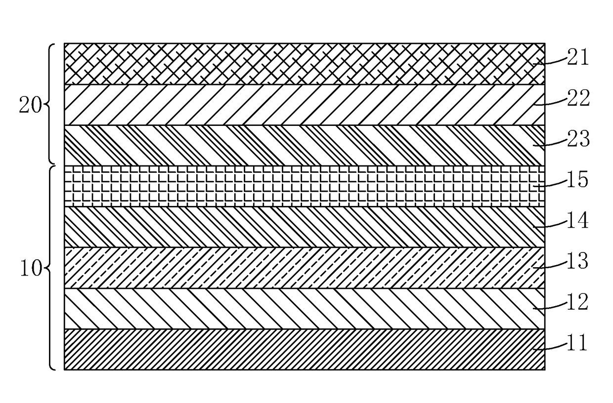
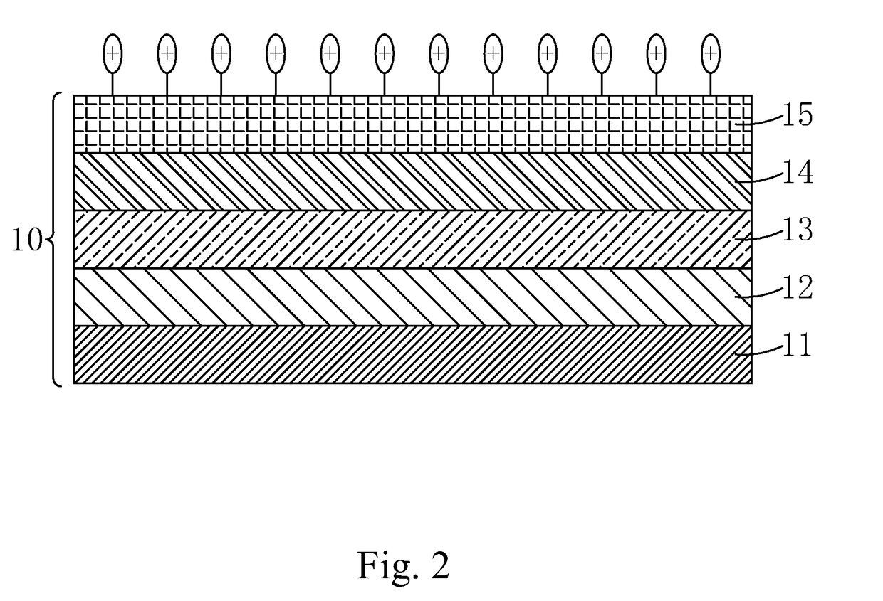
[0026]Step 1: as shown in FIG. 2, providing a thin film transistor (TFT) array substrate 11, forming a cathode 12, an electron transport layer (ETL) 13, a light-emitting layer 14 and a hole transport layer (HTL) 15 sequentially on the TFT array substrate 11 to form a lower substrate 10.

[0027]Wherein, the cathode 12 is a transparent electrode.

[0028]The HTL 15 is made of an organic material with positive radicals.

[0029]Preferably, the positive radicals comprise at least one of NH3+ and H+.

[0030]Specifically, a spin coating process or a spraying process is used to form the ETL 13 on the cathode 12; a spin coating process or an evaporation process is used to form the light-emitting layer 14 on the ETL 13, and a spin coating process or a spraying process is used to form the HTL 15 on the light-emitting layer 15.

[0031]Preferably, the materials of t...


PUM

PropertyMeasurementUnit
temperatureaaaaaaaaaa
transparent conductiveaaaaaaaaaa

Abstract

The invention discloses a transparent OLED display and manufacturing method thereof. The present invention provides a manufacturing method of transparent OLED display, by preparing the cathode and the anode on two different substrates to effectively avoid the destruction of the light-emitting layer made of the organic light-emitting material caused by sputtering the anode at the top of OLED to improve yield rate. The use of the transparent conductive metal oxide to manufacture the cathode and the anode of the OLED display provides an effective solution to the manufacturing of transparent OLED display which requires high conductivity and high transparency for the electrode material. In addition, the two substrates can be manufactured the same time and then pressed to attach to achieve high manufacturing efficiency. The OLED display provided by the present invention is easy to manufacture and provides good performance.

Description

BACKGROUND OF THE INVENTION1. Field of the Invention[0001]The present invention relates to the field of display techniques, and in particular to a transparent OLED display and manufacturing method thereof.2. The Related Arts[0002]The organic light emitting diode (OLED) display, also called organic electroluminescent display, is the new trend of flat panel display technology. Because the OLED display provides the advantages of simple manufacturing process, low cost, low power-consumption, high illumination, wide operating temperature range, thin size, short response time, enabling full-color large display, easy to match integrated circuit (IC) driver, and enabling flexible display, the OLED is recognized as the technology with widest application prospect.[0003]The driving types of OLED can be divided according to the passive matrix OLED (PMOLED) and active matrix OLED (AMOLED), i.e., the direct addressable type and thin film transistor (TFT) addressable type, wherein the AMOLED provi...

Claims


Application Information

Patent Timeline
Patent Type & Authority Applications(United States)
IPC IPC(8): H01L51/00H01L27/32H01L51/52H01L51/50H01L51/56
CPCH01L51/0024H01L27/3244H01L51/0097H01L51/5206H01L51/5234H01L51/5012H01L51/5056H01L51/5072H01L51/5088H01L51/524H01L51/56H01L51/0003H01L51/001H01L51/0021H01L2251/5338H01L2251/308H01L2227/323H01L51/0043H01L51/0039H10K50/00H10K50/81H10K50/82H10K2102/301H10K71/00Y02E10/549Y02P70/50H10K59/123H10K71/50H10K50/15H10K50/17H10K50/828H10K2102/321H10K2102/3031H10K59/12H10K71/164H10K71/12H10K71/60H10K50/841H10K59/1201H10K2102/103H10K2102/311H10K50/11H10K50/16H10K77/111H10K85/115H10K85/151
Inventor XU, CHAO
Owner WUHAN CHINA STAR OPTOELECTRONICS TECH CO LTD
Why Eureka
Try Eureka