
Patsnap Eureka
For R&D, Patsnap Eureka makes reading and utilizing patents & technical documents easy.
Patsnap Eureka AIR
Designed for self-driven R&D workflows. Generate viable solutions, solve complex R&D challenges, empower your innovation with AI.

Patsnap Eureka Materials
Designed for material experts only. Revolutionize your material R&D, from search, analyze, to developing new materials.

TechResearch
Generate reliable direction feasibility study reports for your R&D in just a few steps.

TechSeek
Discover and master advanced knowledge NOW. Basics, ideas, possibilities, all at once.

TechMind
As an expert in R&D Theories, TechMind can generates customized viable solutions instantly.

TechRisk
Analyze your overall solution with one click, know your potential R&D risks in advance.

TechMonitor
Get weekly tech updates, stay abreast of the latest tech innovations and key insights.
Method of synthesizing thickness-controlled graphene through chemical vapor deposition using cu-ni thin film laminate
- Summary
- Abstract
- Description
- Claims
- Application Information
AI Technical Summary
Benefits of technology
Problems solved by technology
Method used
Image

Examples
example 1
of Graphene
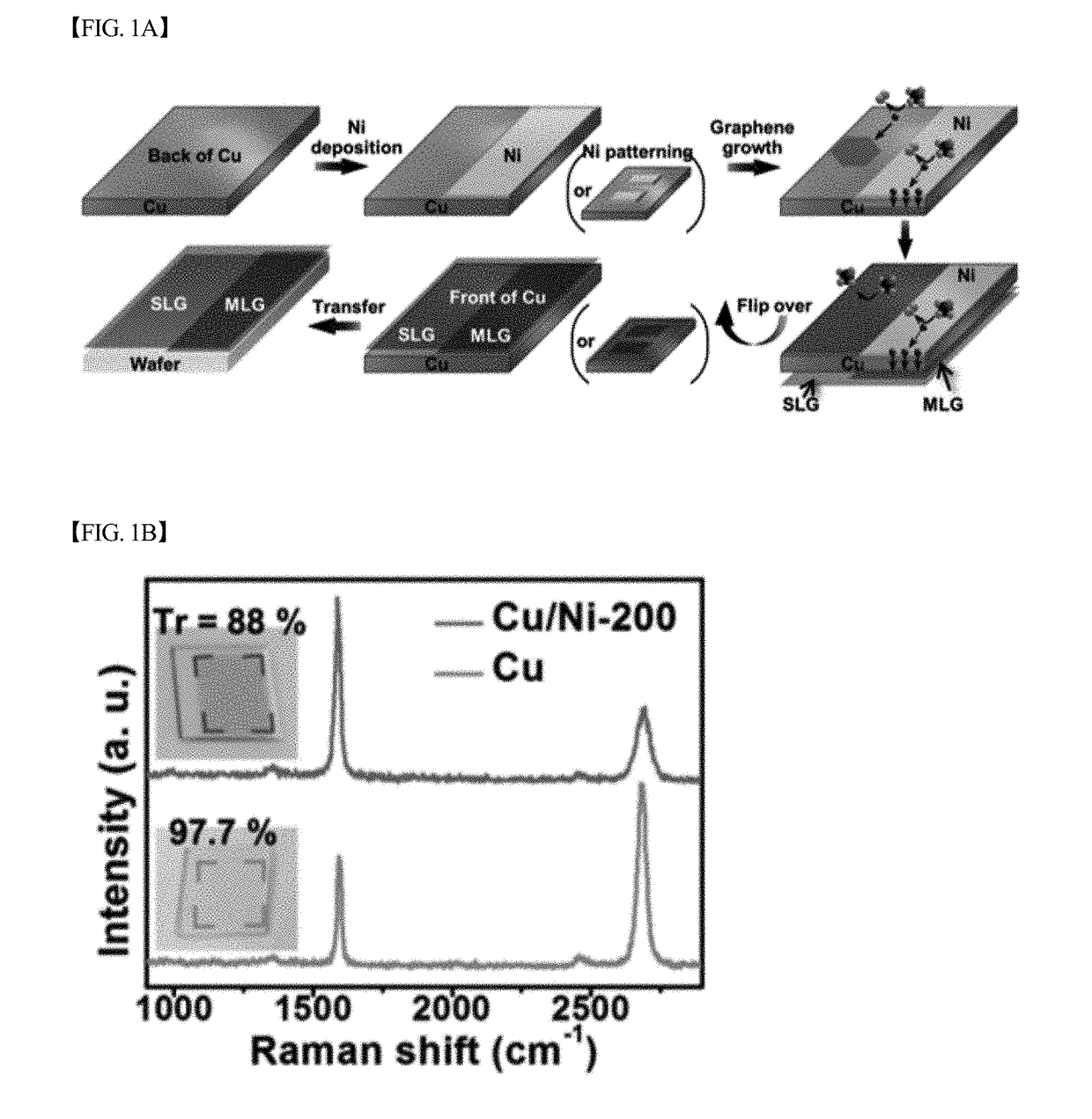
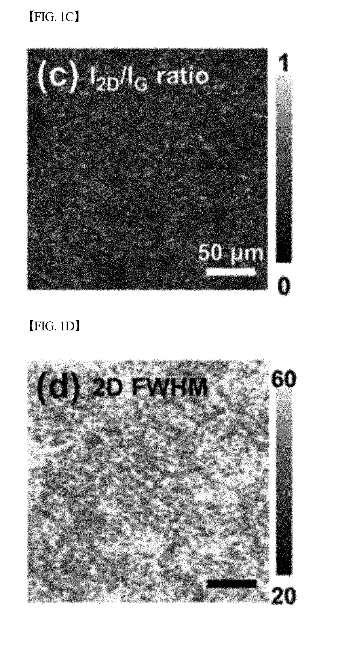
[0072]Thermally deposited on the back surface of a copper thin film having a width of 10 cm, a length of 10 cm, and a height of 25 μm was a nickel thin film having a width of 10 cm, a length of 10 cm, and a thickness of 50 nm. The prepared Cu—Ni thin film laminate was placed in a CVD chamber and heated in the presence of hydrogen. When the temperature of the Cu—Ni thin film laminate reached 1000° C., CH4 was supplied for 20 min at a flow rate of 50 sccm, thereby growing graphene. After the termination of the growth of graphene, the chamber was cooled and the synthesized graphene was transferred onto glass or a silicon dioxide substrate.
examples 2 to 38
phene
[0073]The graphene of each of Examples 2 to 38 was synthesized in the same manner as in Example 1, with the exception that the conditions of Examples 2 to 38 were used in lieu of the conditions of Example 1 of Table 1 below.
example 39
of Patterned Graphene
[0074]The patterned graphene of Example 39 was synthesized in the same manner as in Example 1, with the exception that the conditions of Example 39 were used in lieu of the conditions of Example 1 of Table 1 below and that a nickel thin film having the pattern shown in FIG. 1E was deposited in lieu of the nickel thin film of Example 1 having a width of 10 cm, a length of 10 cm, and a thickness of 50 nm.
Example 40: Synthesis of FeCl3-Doped Graphene
[0075]The FeCl3-doped graphene of Example 40 was synthesized in a manner in which the graphene transferred onto the glass or silicon substrate of Example 30 was placed in a vacuum chamber together with a crucible containing a FeCl3 powder, after which Ar was supplied at a flow rate of 10 sccm, heated at 350° C. for 5 hr, and rapidly cooled.
Example 41: Synthesis of FeCl3-Doped Graphene
[0076]The FeCl3-doped graphene of Example 41 was synthesized in the same manner as in Example 40, with the exception that the graphene of ...
PUM
| Property | Measurement | Unit |
|---|---|---|
| Temperature | aaaaa | aaaaa |
| Time | aaaaa | aaaaa |
| Thickness | aaaaa | aaaaa |
Abstract
Description
Claims
Application Information
 - R&D Engineer
- R&D Manager
- IP Professional
- Industry Leading Data Capabilities
- Powerful AI technology
- Patent DNA Extraction
Browse by: Latest US Patents, China's latest patents, Technical Efficacy Thesaurus, Application Domain, Technology Topic, Popular Technical Reports.
© 2024 PatSnap. All rights reserved.Legal|Privacy policy|Modern Slavery Act Transparency Statement|Sitemap|About US| Contact US: help@patsnap.com