Electronic circuit package using composite magnetic sealing material

a technology of composite magnetic sealing and electronic circuits, applied in the direction of coatings, basic electric elements, other domestic articles, etc., can solve the problems of conventional composite magnetic sealing materials, difficult to solve malfunction and radio disturbance, difficult to etc., to prevent substrate warpage, easy and reliably connect metal films to power supply patterns, small thermal expansion coefficient

Inactive Publication Date: 2019-01-31
TDK CORPARATION
View PDF19 Cites 11 Cited by
  • Summary
  • Abstract
  • Description
  • Claims
  • Application Information

AI Technical Summary

Benefits of technology

[0020]Preferably, in the present invention, the metal film is mainly composed of at least one metal selected from a group consisting of Au, Ag, Cu, and Al, and more preferably, the surface of the metal film is covered with an antioxidant film. In the present invention, it is preferable that the power supply pattern is exposed to a side surface of the substrate and that the metal film contacts the exposed power supply pattern. With this configuration, it is possible to easily and reliably connect the metal film to the power supply pattern.
[0021]As described above, the electronic circuit package according to the present invention includes the magnetic mold resin having a small thermal expansion coefficient. Thus, it is possible to prevent the warp of the substrate, interfacial delamination or crack of a molding material with obtaining the magnetic shielding characteristics.

Problems solved by technology

However, this tendency poses a problem of malfunction and radio disturbance due to noise.
The problem of malfunction and radio disturbance is difficult to be solved by conventional noise countermeasure techniques.
However, conventional composite magnetic sealing materials have a drawback in that it has a large thermal expansion coefficient.
Thus, a mismatch occurs between a composite magnetic sealing material and a package substrate or electronic components in terms of the thermal expansion coefficient.
As a result, an aggregated substrate having a strip shape after molding may be greatly warped, or there may occur a warp large enough to cause a problem with connectivity of an electronic circuit package in a diced state in mounting reflow.
On the other hand, the difference in physical properties between semiconductor ICs and electronic components mounted on a substrate and a molding material also generates a stress, causing various problems such as interfacial delamination of the molding material and crack of the electronic components or molding material.
H10-64714, the composite magnetic sealing material obtained by adding general soft magnetic powder to a mold resin cannot achieve a target small thermal expansion coefficient.

Method used


Image

  • Electronic circuit package using composite magnetic sealing material
  • Electronic circuit package using composite magnetic sealing material
  • Electronic circuit package using composite magnetic sealing material

Examples


first embodiment

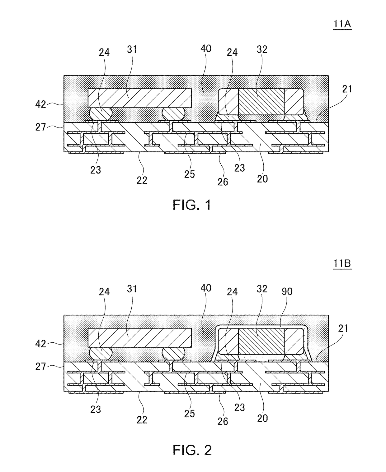
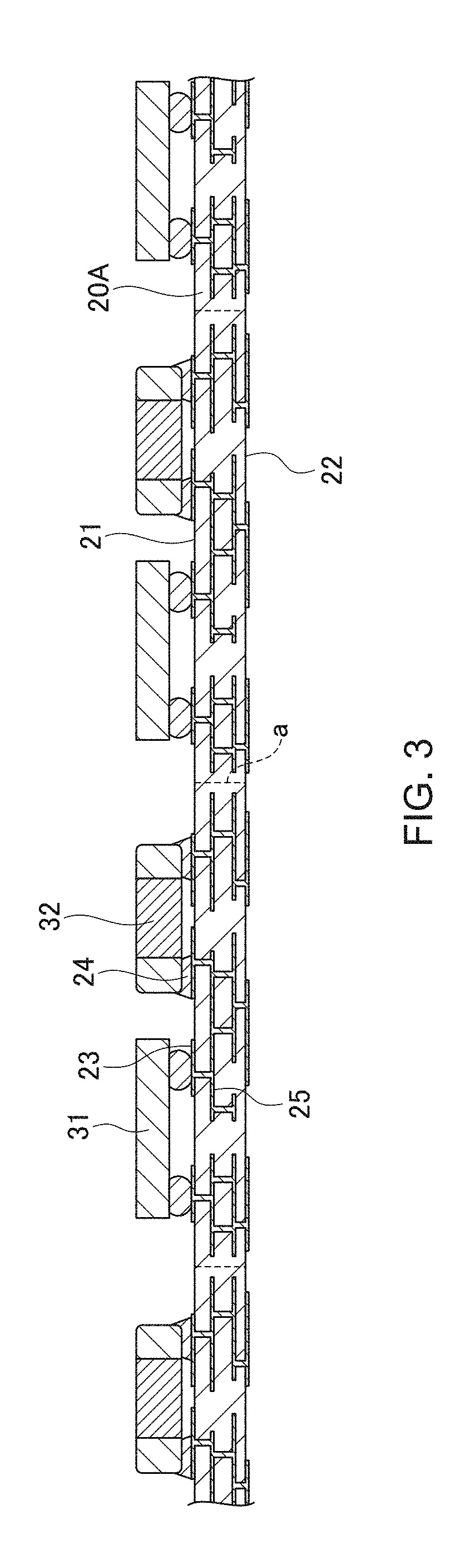
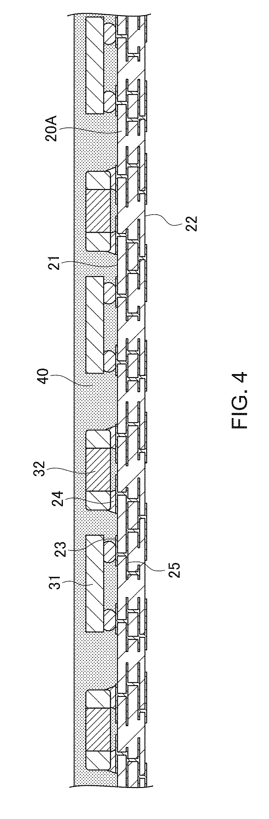
[0063]FIG. 1 is a cross-sectional view illustrating a configuration of an electronic circuit package 11A according to the first embodiment of the present invention.

[0064]As illustrated in FIG. 1, the electronic circuit package 11A according to the present embodiment includes a substrate 20, a plurality of electronic components 31 and 32 mounted on the substrate 20, and a magnetic mold resin 40 covering a front surface 21 of the substrate 20 so as to embed the electronic components 31 and 32.

[0065]Although the type of the electronic circuit package 11A according to the present embodiment is not especially limited, examples thereof include a high-frequency module handling a high-frequency signal, a power supply module performing power supply control, an SIP (System-In-Package) having a 2.5D structure or a 3D structure, and a semiconductor package for radio communication or digital circuit. Although only two electronic components 31 and 32 are illustrated in FIG. 1, more electronic com...

second embodiment

[0106]FIG. 15 is a cross-sectional view illustrating a configuration of an electronic circuit package 12A according to the second embodiment of the present invention.

[0107]As illustrated in FIG. 15, an electronic circuit package 12A according to the present embodiment differs from the electronic circuit package 11A according to the first embodiment illustrated in FIG. 1 in that a planar size of the magnetic mold resin 40 is slightly smaller than a planar size of the substrate 20 and, therefore, an outer peripheral portion of the front surface 21 of the substrate is exposed from the magnetic mold resin 40. Other configurations are the same as those of the electronic circuit package 11A according to the first embodiment. Thus, in FIG. 15, the same reference numerals are given to the same elements as in FIG. 1, and repetitive descriptions will be omitted.

[0108]As exemplified by the electronic circuit package 12A according to the present embodiment, it is not essential in the present in...

third embodiment

[0113]FIG. 19 is a cross-sectional view illustrating a configuration of an electronic circuit package 13A according to the third embodiment of the present invention.

[0114]As illustrated in FIG. 19, the electronic circuit package 13A according to the present embodiment differs from the electronic circuit package 11A in that it further includes a metal film 60 that covers an upper surface 41 and a side surface 42 of the magnetic mold resin 40 and covers a side surface 27 of the substrate 20. Out of the internal wirings 25 illustrated in FIG. 19, internal wirings 25G are power supply patterns. A part of the power supply patterns 25G is exposed from the substrate 20 on the side surface 27. The power supply patterns 25G are typically ground patterns to which a ground potential is to be applied; however, it is not limited to the ground patterns as long as the power supply patterns 25G are a pattern to which a fixed potential is to be applied. Other configurations are the same as those of ...


PUM

PropertyMeasurementUnit
thicknessaaaaaaaaaa
volume resistivityaaaaaaaaaa
thicknessaaaaaaaaaa

Abstract

Disclosed herein is an electronic circuit package includes a substrate, an electronic component mounted on a surface of the substrate, a magnetic mold resin covering the surface of the substrate so as to embed therein the electronic component, a metal film covering the magnetic mold resin, and a magnetic film covering the metal film. The magnetic mold resin includes a resin material, and a magnetic filler blended in the resin material, the magnetic filler containing Fe and 32 wt. % or more and 39 wt. % or less of a metal material composed mainly of Ni.

Description

BACKGROUND OF THE INVENTIONField of the Invention[0001]The present invention relates to an electronic circuit package and, more particularly, to an electronic circuit package using a composite magnetic sealing material.Description of Related Art[0002]In recent years, an electronic device such as a smartphone is equipped with a high-performance radio communication circuit and a high-performance digital chip, and an operating frequency of a semiconductor IC used therein tends to increase. Further, adoption of an SIP (System-In Package) having a 2.5D or 3D structure, in which a plurality of semiconductor ICs are connected by a shortest wiring, is accelerated, and modularization of a power supply system is expected to accelerate. Further, an electronic circuit module having a large number of modulated electronic components (collective term of components, such as passive components (an inductor, a capacitor, a resistor, a filter, etc.), active components (a transistor, a diode, etc.), in...

Claims


Application Information

Patent Timeline
Patent Type & Authority Applications(United States)
IPC IPC(8): H01L23/552B29C45/14H01L23/31H01L23/498H01L23/00H01L23/29B29L31/00H01L21/56
CPCH01L24/16H01L23/49822B29K2995/0008H01L23/295B29C45/14655H01L21/561H01L2224/16104H01L23/552B29L2031/712H01L23/3114H01L24/97H01L21/565H01L2224/97H01L23/3121B29C45/14336H01L2924/15159H01L2924/19041H01L2224/16227H01L2924/19105H01L2924/15192H01L2224/131H01L2924/3511H01L2924/15313H01L2924/19042H01L2924/3025H01L2224/81H01L2924/014H01L2924/00014B29C45/0001B29L2031/3481H01L24/13H01L24/81H01L25/16H01L2224/13101H01L2224/16225H01L2924/181H01L2924/00012
Inventor KAWABATA, KENICHI
Owner TDK CORPARATION
Why Eureka
Try Eureka