Coated electrical assembly
a technology of electrical components and coatings, applied in the direction of coatings, non-metallic protective coating applications, printed circuit non-printed electric components association, etc., can solve the problems of time-consuming and expensive deposition process, high starting material cost, etc., and achieve excellent moisture-barrier properties, high level of chemical, electrical and physical protection, and high level of waterproofing
- Summary
- Abstract
- Description
- Claims
- Application Information
AI Technical Summary
Benefits of technology
Problems solved by technology
Method used
Image
Examples
example 1
Deposition of a Single SiOxCyHz Layer Using Ar as Non-Reactive Gas
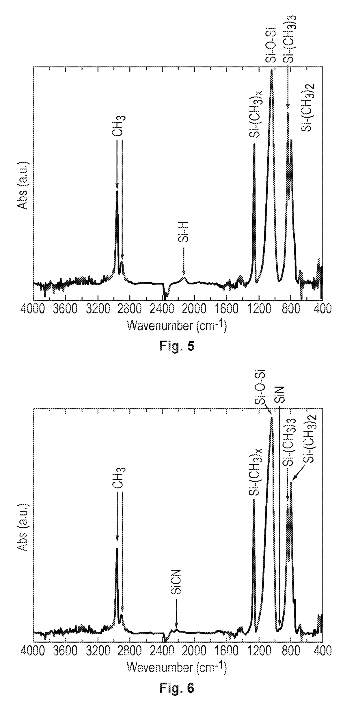
[0135]An electrical assembly was placed into a plasma-enhanced chemical vapour deposition (PECVD) deposition chamber, and the pressure was then brought to ˜10−2 mbar. Hexamethyldisiloxane (HMDSO) and Ar were injected at a flow rate of 17.5 sccm and 20 sccm respectively. Pressure was allowed to stabilize and plasma was ignited at a RF power density of 0.057 Wcm−2, resulting in a process pressure of 0.140 mbar. The process was run for 10 minutes.
[0136]Polymeric organosilicon SiOxCyHz layers were obtained on the electrical assembly. The FTIR transmission spectrum for the deposited layer is shown in FIG. 5.
[0137]The SiOxCyHz layers showed hydrophobic character with a WCA (water contact angle) of ˜100°.
[0138]Coating adhesion to electrical assembly was tested on a PCB substrate by means of tape peel test resulting in coating good adhesion on both solder mask and metal substrate surfaces (i.e. no coating peeled off the solde...
example 2
Deposition of Single SiOxCyHzNa Layer Using N2O as Reactive Gas
[0139]An electrical assembly was placed into a PECVD deposition chamber, and the pressure was then brought to ˜10−2 mbar. HMDSO and N2O were injected at a flow rate of 17.5 sccm and 30 sccm respectively. Pressure was allowed to stabilize and plasma was ignited at a RF power density of 0.057 Wcm−2, resulting in a process pressure of 0.160 mbar. The process was run for 10 minutes.
[0140]Polymeric organosilicon SiOxCyHzNa layers were obtained on the electrical assembly. The FTIR transmission spectrum for the deposited layer is shown in FIG. 6.
[0141]The SiOxCyHz layers showed hydrophobic character with a WCA (water contact angle) of ˜95°.
example 3
Deposition of Single SiOxCyHzNa Layer Using NH3 as Reactive Gas and Ar as Non-Reactive Gas
[0142]An electrical assembly was placed into a PECVD deposition chamber, and the pressure was then brought to ˜10−2 mbar. HMDSO, NH3 and Ar were injected at a flow rate of 4.4 sccm, 80 sccm and 20 sccm respectively. Pressure was allowed to stabilize and plasma was ignited at a RF power density of 0.057 Wcm−2, resulting in a process pressure of 0.120 mbar. The process was run for 30 minutes.
[0143]Polymeric organosilicon SiOxCyHzNa layers were obtained on the electrical assembly. The FTIR transmission spectrum for the deposited layer is shown in FIG. 7.
PUM
| Property | Measurement | Unit |
|---|---|---|
| pressure | aaaaa | aaaaa |
| pressure | aaaaa | aaaaa |
| pressure | aaaaa | aaaaa |
Abstract
Description
Claims
Application Information


