Organic light-emitting diode device and compound for charge generation layer included therein

a technology of light-emitting diodes and charge generation layers, which is applied in the direction of group 3/13 element organic compounds, organic chemistry, chemistry apparatus and processes, etc., can solve the problems of reducing the power efficiency and lifespan of organic light-emitting diodes, and achieves long lifespan characteristics, low driving voltage, and high efficiency

Active Publication Date: 2019-09-19
SAMSUNG DISPLAY CO LTD
View PDF0 Cites 4 Cited by
  • Summary
  • Abstract
  • Description
  • Claims
  • Application Information

AI Technical Summary

Benefits of technology

[0007]Exemplary embodiments of the present disclosure are directed to an organic light-emitting diode device having low driving voltage, high efficiency, and long lifespan characteristics by including a charge generation layer having an excellent ability to generate and transfer charges.

Problems solved by technology

However, a conventional charge generation layer is problematic in that it increases the driving voltage of the tandem-type (or tandem kind) of light-emitting device by about 1.3-2 times or more compared to that of a conventional single-type (or single kind) of organic light-emitting diode device due to its poor ability to generate and transfer charges, thus reducing the power efficiency and lifespan of the organic light-emitting diode device.

Method used


Image

  • Organic light-emitting diode device and compound for charge generation layer included therein
  • Organic light-emitting diode device and compound for charge generation layer included therein
  • Organic light-emitting diode device and compound for charge generation layer included therein

Examples


example 1

on of Organic Light-Emitting Diode Device Formation of Hole Transport Region

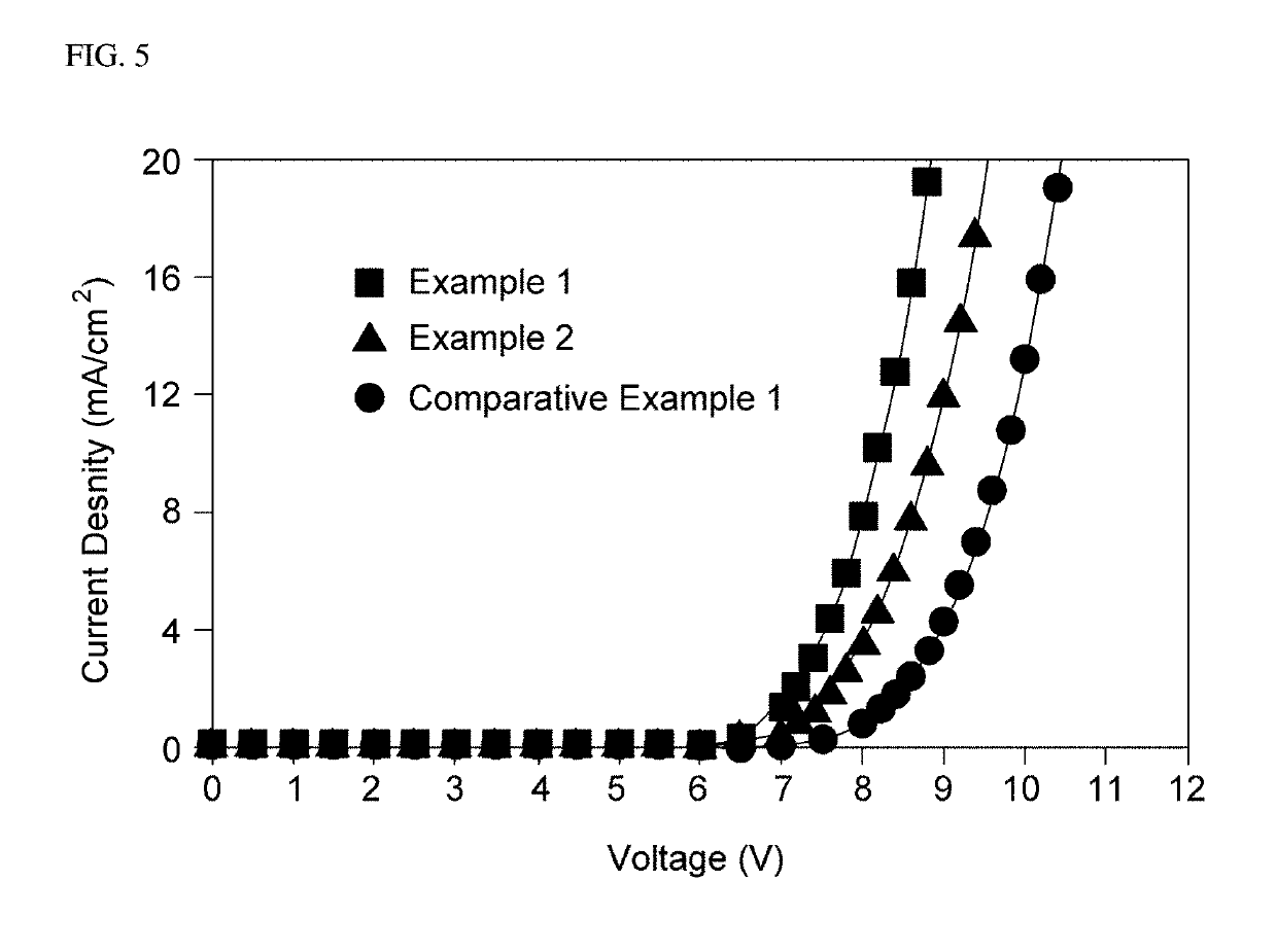
[0165]A glass substrate having formed thereon a 15 Ω / cm2 (120 nm) ITO (Corning) as an anode was cut to a size of 50 mm×50 mm×0.5 mm, and washed by ultrasonic cleaning for 15 minutes with each of acetone, isopropyl alcohol, and purified water. Next, the glass substrate was irradiated with UV light for 30 minutes, washed by exposure to ozone, and then placed in a vacuum deposition system.

[0166]On the ITO anode, m-TDATA and F4-TCNQ (3 wt %) were co-deposited to form a 20 nm-thick hole injection layer. Next, on the hole injection layer, NPB was deposited to form a 150 nm-thick hole transport layer, thereby forming a hole transport region.

Formation of First Light-Emitting Unit

[0167]On the hole transport region, ADN and DPAVBi (5 wt %) were co-deposited to form a 20 nm-thick light-emitting layer. Next, on the light-emitting layer, Bphen was deposited to form a 30 nm-thick electron transport (ET)-auxiliary light em...

example 2

on of Organic Light-Emitting Diode Device

[0172]An organic light-emitting diode device of Example 2 was fabricated in substantially the same manner as described in Example 1, except that the charge generation layer was formed using the boron-containing compound and the metal halide at a weight ratio of 20:80.


PUM

PropertyMeasurementUnit
work functionaaaaaaaaaa
chargeaaaaaaaaaa
charge-transferaaaaaaaaaa

Abstract

Disclosed is an organic light-emitting diode device including: a first electrode; a second electrode disposed opposite to the first electrode; m light-emitting units (where m is an integer of 2 or more) disposed between the first electrode and the second electrode, and including at least one light-emitting layer; and m-1 charge generation layers each interposed between two adjacent light-emitting units of the m light-emitting units; wherein at least one of the m-1 charge generation layers includes a compound for a charge generation layer, which includes a boron-containing compound bonded to a metal halide by a one-electron sigma bond.

Description

CROSS-REFERENCE TO RELATED APPLICATION[0001]This application claims priority to and the benefit of Korean Patent Application No. 10-2018-0029112, filed on Mar. 13, 2018, in the Korean Intellectual Property Office (KIPO), the entire content of which is incorporated herein by reference.BACKGROUND1. Field[0002]Exemplary embodiments of the present disclosure relate to an organic light-emitting diode device having low driving voltage, high efficiency, and long lifespan characteristics, and a compound for a charge generation layer included in the device, which has excellent charge-generation ability and charge-transfer ability.2. Discussion of Related Art[0003]An organic light-emitting display device is a self-luminescent display device that displays images by means of a plurality of organic light-emitting diodes configured to emit light. This organic light-emitting display device exhibits characteristics, such as low power consumption, high luminance, and high response speed, and is thus...

Claims


Application Information

Patent Timeline
Patent Type & Authority Applications(United States)
IPC IPC(8): H01L51/00C07F5/02
CPCH01L51/0051H01L51/5044H01L51/008C07F5/025H01L51/5278H10K85/322H10K50/80H10K50/00H10K85/611H10K85/654H10K50/19H10K85/657H10K50/11H10K50/131
Inventor CHO, YOONHYEUNGJANG, HYUNGSEOKKIM, DONGCHANKIM, WONJONGMOON, JIYOUNGPARK, YEONGRONGSEO, DONGKYUYEO, MYUNGCHULLEE, JIHYE
Owner SAMSUNG DISPLAY CO LTD
Why Eureka
Try Eureka