LED module
- Summary
- Abstract
- Description
- Claims
- Application Information
AI Technical Summary
Benefits of technology
Problems solved by technology
Method used
Image


Examples
first embodiment
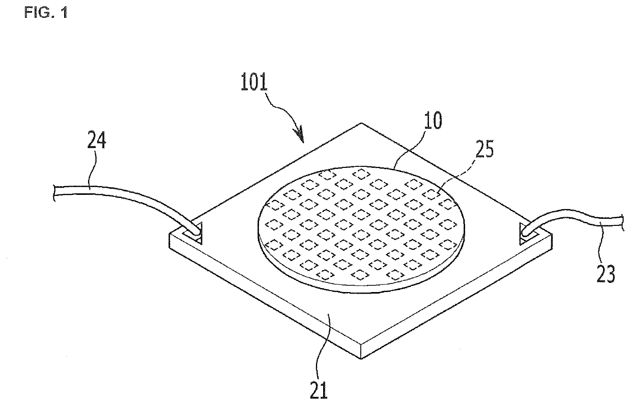
[0034]Referring to FIGS. 1 and 2, an LED module 101 includes a substrate 21, an LED bare chip 25, and a color conversion sheet 10.
[0035]The substrate 21 can be any substrate that can mount the LED bare chip 25 at a high density. Although not limited, for example, such a substrate 21 may include alumina, quartz, calcium zirconate, forsterite, SIC, graphite, fused silica, mullite, cordierite, zirconia, beryllia, aluminum nitride, low temperature co-fired ceramic (LTCC), and the like.
[0036]The substrate 21 may be formed of a straight, circular or polygonal plate, and a first wire 23 and a second wire 24 for supplying power to the LED bare chip 25 are installed on the substrate 21. In the LED module 101 according to the first embodiment, the LED bare chip 25 and the substrate 21 are electrically connected with each other via a soldering portion 27 and the LED module 101 does not have a separate bonding wire. The soldering portion 27 electrically connects the LED bare chip 25 and the su...
second embodiment
[0051]The LED module 102 according to the present invention further includes an underfilling layer 22a. The underfilling layer 22a is formed to fill a space between the LED bare chips 25 on the substrate and to cover the periphery of the LED bare chip. The underfilling layer 22a may be formed by attaching a sheet made of a film having elasticity to the substrate or by injecting a liquid resin between the LED bare chips 25. The underfilling layer 22a may also be made of at least one of an epoxy resin, a polyimide resin, a UV curable resin as a transparent adhesive component, a thermosetting resin, and a sealant.
[0052]In addition, the underfilling layer 22a may be formed of a light-transmitting material that transmits light and may be formed of a white or silver material that reflects light. One underfilling layer 22a is in contact with a side surface of the plurality of LED bare chips 25 to be formed of a unibody or a plurality of underfilling layers 22a may be formed individually on...
third embodiment
[0061]In the third embodiment, the light diffusion adhesive layer 22b is formed to fill the space between the LED bare chips 25. The light diffusion adhesive layer 22b is preferably formed in a film shape having elasticity for firm adhesion with the color conversion sheet 10 to be described below. At this time, the light diffusion adhesive layer 22b is made of a light transmitting material that transmits light, and a surface where the light diffusion adhesive layer 22b contacts the substrate may be further applied with a white or silver material for reflecting light. However, the light diffusion adhesive layer 22b may be formed by injecting a liquid resin into the LED bare chips 25. At this time, the light diffusion adhesive layer 22b may be made of an epoxy resin or a polyimide resin.
[0062]The light diffusion adhesive layer 22b is formed to cover the side surface of the LED bare chip 25. More specifically, the light diffusion adhesive layer 22b may be formed to be in contact with t...
PUM
 Abstract
Description
Claims
Application Information