Multijunction solar cell and solar cell assemblies for space applications

a solar cell and multi-junction technology, applied in the field of solar cells and the fabrication of solar cells, can solve the problems of increasing the complexity of properly specifying and manufacturing, affecting the efficiency of solar cells, and affecting the performance of solar cells. achieve the effect of optimizing such efficiency, increasing the efficiency of multi-junction solar cells, and increasing photoconversion efficiency

Inactive Publication Date: 2020-01-23
SOLAERO TECH CORP
View PDF0 Cites 20 Cited by
  • Summary
  • Abstract
  • Description
  • Claims
  • Application Information

AI Technical Summary

Benefits of technology

[0039]It is an object of the present disclosure to provide increased photoconversion efficiency in a multijunction solar cell for space applications over the operational life of the photovoltaic power system.
[0040]It is another object of the present disclosure to provide in a multijunction solar cell in which the composition of the subcells and their band gaps has been configured to maximize the efficiency of the solar cell at operational conditions of a predetermined high temperature (specifically, in the range of 40 to 70 degrees Centigrade) in deployment in space at AM0 one-sun solar spectrum at a predetermined time after the initial deployment, such time being at least one, five, ten, fifteen or twenty years and not at the time of initial deployment.
[0041]It is another object of the present disclosure to provide in a multijunction solar cell in which the composition of the subcells and their band gaps maximizes the efficiency of the solar cell at a predetermined high temperature (in the range of 40 to 70 degrees Centigrade) in deployment in space at AM0 at a predetermined time after the initial deployment, such time being at least one year.

Problems solved by technology

Compared to silicon, III-V compound semiconductor multijunction devices have greater energy conversion efficiencies and are generally more radiation resistance, although they tend to be more complex to properly specify and manufacture.
Such rigorous testing and qualifications are not generally applicable to terrestrial solar cells and solar cell arrays.
The space solar cells and arrays experience a variety of complex environments in space missions, including the vastly different illumination levels and temperatures seen during normal earth orbiting missions, as well as even more challenging environments for deep space missions, operating at different distances from the sun, such as at 0.7, 1.0 and 3.0 AU (AU meaning astronomical units).
The photovoltaic arrays also endure anomalous events from space environmental conditions, and unforeseen environmental interactions during exploration missions.
Hence, electron and proton radiation exposure, collisions with space debris, and / or normal aging in the photovoltaic array and other systems could cause suboptimal operating conditions that degrade the overall power system performance, and may result in failures of one or more solar cells or array strings and consequent loss of power.
Such precautions are generally unnecessary in terrestrial applications.
In summary, it is evident that the differences in design, materials, and configurations between a space-qualified III-V compound semiconductor solar cell and subassemblies and arrays of such solar cells, on the one hand, and silicon solar cells or other photovoltaic devices used in terrestrial applications, on the other hand, are so substantial that prior teachings associated with silicon or other terrestrial photovoltaic system are simply unsuitable and have no applicability to the design configuration of space-qualified solar cells and arrays.
Charged particles in space could lead to damage to solar cell structures, and in some cases, dangerously high voltage being established across individual devices or conductors in the solar array.
These large voltages can lead to catastrophic electrostatic discharging (ESD) events.
However, in reality, changing a material parameter that increases the voltage may result in a decrease in current, and therefore a lower power output.
Such material design parameters are interdependent and interact in complex and often unpredictable ways, and for that reason are not “result effective” variables that those skilled in the art confronted with complex design specifications and practical operational considerations can easily adjust to optimize performance.
Although the various electrical contributions to the Fill Factor such as series resistance, shunt resistance, and ideality (a measure of how closely the semiconductor diode follows the ideal diode equation) may be theoretically understood, from a practical perspective the actual Fill Factor of a given subcell cannot always be predicted, and the effect of making an incremental change in composition or band gap of a layer may have unanticipated consequences and effects on the solar subcell semiconductor material, and therefore an unrecognized or unappreciated effect on the Fill Factor.
Thus, the Voc and Jsc parameters, either alone or in combination, are not necessarily “result effective” variables that those skilled in the art confronted with complex design specifications and practical operational considerations can easily adjust to optimize performance.
Furthermore, the fact that the short circuit current density (Jsc), the open circuit voltage (Voc), and the fill factor (FF), are affected by the slightest change in such design variables, the purity or quality of the chemical pre-cursors, or the specific process flow and fabrication equipment used, and such considerations further complicates the proper specification of design parameters and predicting the efficiency of a proposed design which may appear “on paper” to be advantageous.
Here again there are trade-offs between including specific elements in the composition of a layer which may result in improved voltage associated with such subcell and therefore potentially a greater power output, and deviation from exact crystal lattice matching with adjoining layers as a consequence of including such elements in the layer which may result in a higher probability of defects, and therefore lower manufacturing yield.
Mismatches in the lattice constants create defects or dislocations in the crystal lattice where recombination centers can occur to cause the loss of photogenerated minority carriers, thus significantly degrading the photovoltaic quality of the device.

Method used


Image

  • Multijunction solar cell and solar cell assemblies for space applications
  • Multijunction solar cell and solar cell assemblies for space applications
  • Multijunction solar cell and solar cell assemblies for space applications

Examples


first embodiment

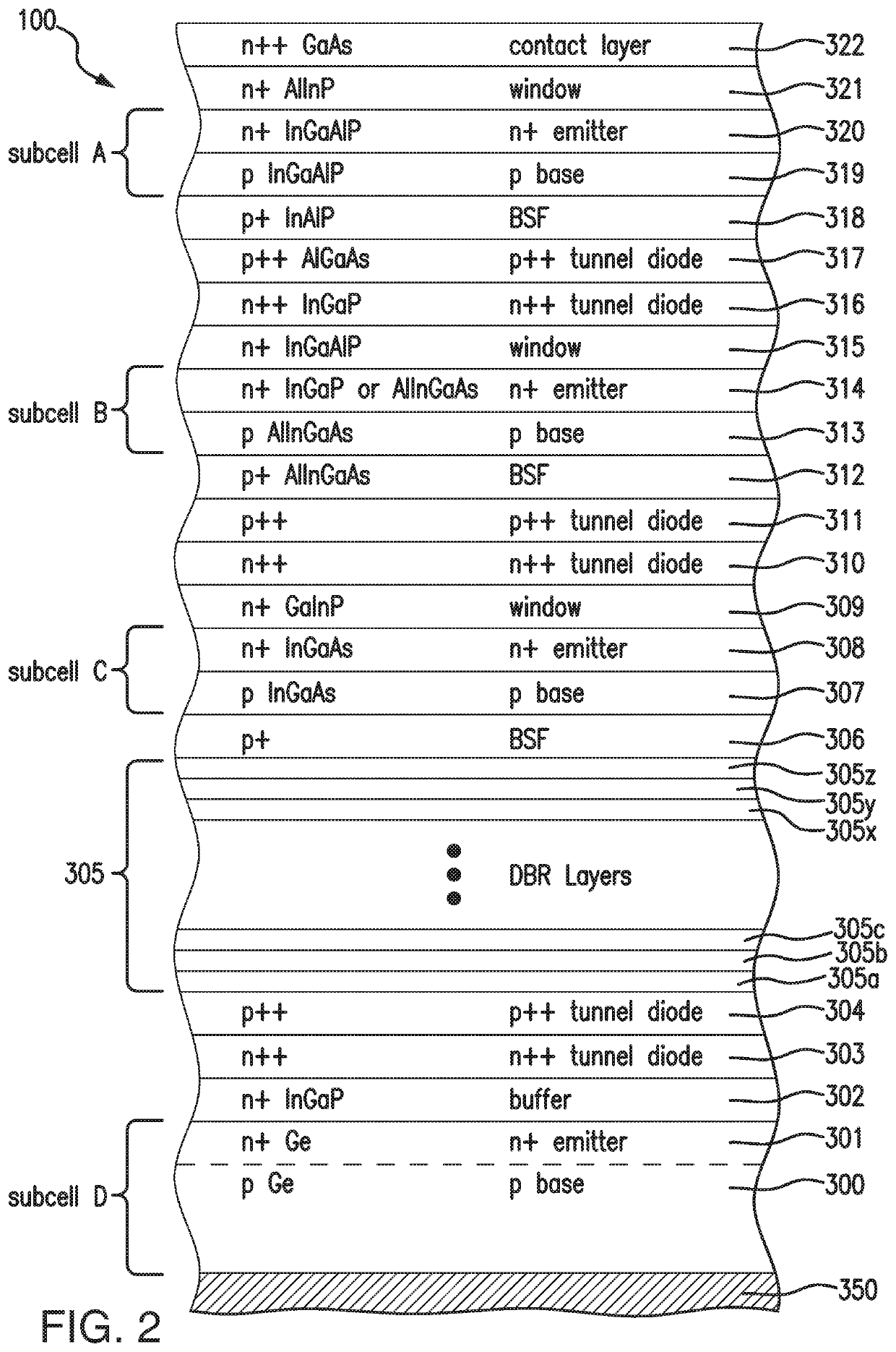
[0166]Turning to the multijunction solar cell device of the present disclosure, FIG. 2 is a cross-sectional view of a four junction solar cell 100 after several stages of fabrication including the growth of certain semiconductor layers on the growth substrate up to the contact layer 322 as presented in to the disclosure of parent application Ser. No. 15 / 873,135 filed Jan. 17, 2018.

[0167]As shown in the illustrated example of FIG. 2, the bottom or fourth subcell D includes a growth substrate 300 formed of p-type germanium (“Ge”) which also serves as a base layer. A back metal contact pad 350 formed on the bottom of base layer 300 provides the bottom p type polarity electrical contact to the multijunction solar cell 100. The bottom subcell D, further includes, for example, a highly doped n-type Ge emitter layer 301, and an n-type indium gallium arsenide (“InGaAs”) nucleation layer 302. The nucleation layer is deposited over the base layer, and the emitter layer 301 is formed in the su...

second embodiment

[0204]FIG. 4B depicts an upright metamorphic multijunction solar cell 400 grown on an n type germanium substrate 390. Although the depicted embodiment is a five junction solar cell with three lattice matched upper subcells A, B, C which are lattice mismatched from lower germanium subcells D and E, in other embodiments there may be two lattice matched upper subcells, and / or one lower germanium subcell. The lattice constant graph on the left-hand side of the Figure depicts the change in lattice constant through the thickness of the solar cell.

[0205]In FIG. 4B various subcells are similar to the structure described and depicted in FIG. 4A and in the interest of brevity, the description of layers 405 to 409, and 306 through 322 will not be repeated here.

[0206]Since in this embodiment, the growth substrate 390 does not include a photovoltaic junction, a tunnel diode consisting of an n++ layer 391 is grown directly over the growth substrate 390, and a p++ layer 392 of the tunnel diode is ...

embodiment 4

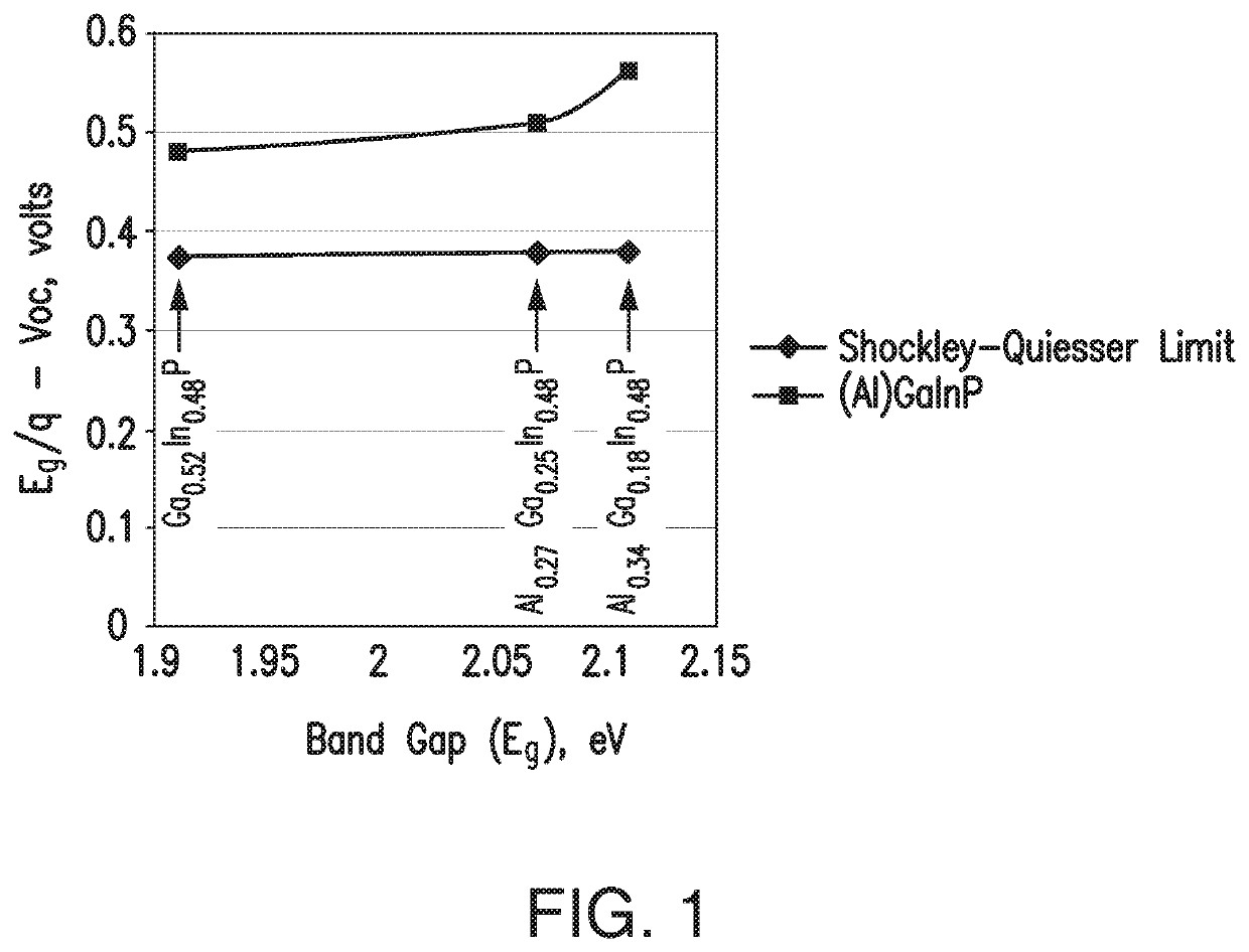
[0266]Although the differences in band gap among the various embodiments described above, i.e., of the order of 0.1 to 0.2 eV, may seem relatively small, it is evident that such adjustments result in an increase in the EOL solar cell efficiency from 24.4% as reported in the parent application U.S. patent application Ser. No. 14 / 828,206 filed Aug. 17, 2015 (and corresponding published European Patent Application EP 3 133 650 A1) to 25.7% for the solar cell of embodiment 4 described above, which is certainly a surprising and unexpected improvement that would constitute an “inventive step” over the related configuration described in the parent application and European patent application publication.

[0267]The wide range of electron and proton energies present in the space environment necessitates a method of describing the effects of various types of radiation in terms of a radiation environment which can be produced under laboratory conditions. The methods for estimating solar cell deg...


PUM

PropertyMeasurementUnit
band gapaaaaaaaaaa
band gapaaaaaaaaaa
band gapaaaaaaaaaa

Abstract

A multijunction solar cell having an upper first solar subcell composed of a semiconductor material having a first band gap; a second solar subcell adjacent to said first solar subcell and composed of a semiconductor material having a second band gap smaller than the first band gap and being lattice matched with the upper first solar subcell; a third solar subcell adjacent to said second solar subcell and composed of a semiconductor material having a third band gap smaller than the second band gap and being lattice matched with the second solar subcell; a fourth solar subcell adjacent to and lattice mismatched from said third solar subcell and composed of germanium grown on a growth substrate. In some embodiments of a five junction solar cell, the growth substrate forms a bottom solar subcell and is composed of germanium.

Description

REFERENCE TO RELATED APPLICATIONS[0001]This application is a continuation-in-part of U.S. patent application Ser. No. 15 / 873,135 filed Jan. 17, 2018, which in turn is a continuation-in-part of U.S. patent application Ser. No. 14 / 828,206, filed Aug. 17, 2015.[0002]This application is related to co-pending U.S. patent application Ser. No. 14 / 660,092 filed Mar. 17, 2015, which is a division of U.S. patent application Ser. No. 12 / 716,814 filed Mar. 3, 2010, now U.S. Pat. No. 9,018,521; which was a continuation in part of U.S. patent application Ser. No. 12 / 337,043 filed Dec. 17, 2008.[0003]This application is also related to co-pending U.S. patent application Ser. No. 13 / 872,663 filed Apr. 29, 2013, which is also a continuation-in-part of application Ser. No. 12 / 337,043, filed Dec. 17, 2008.[0004]This application is also related to U.S. patent application Ser. No. 14 / 828,197, filed Aug. 17, 2015.[0005]All of the above related applications are incorporated herein by reference in their en...

Claims


Application Information

Patent Timeline
Patent Type & Authority Applications(United States)
IPC IPC(8): H01L31/02H01L31/056H01L31/05H01L31/047H01L31/0687
CPCH01L31/056H01L31/047H01L31/0508H01L31/06875H01L31/02008H01L31/03046H01L31/048H01L31/0504H01L31/078H01L31/041H01L31/054Y02E10/52Y02E10/544Y02P70/50
Inventor DERKACS, DANIELBITTNER, ZACHARYHART, JOHN
Owner SOLAERO TECH CORP
Why Eureka
Try Eureka