Multiple silicon atom quantum dot and devices inclusive thereof

a quantum dot and silicon atom technology, applied in the field of multi-dangling bonds, can solve the problems of difficult to overcome limitations, difficult to direct observation of mechanically induced covalent bonding of two different atoms using nc-afm, and difficult to overcome challenges preventing practical applications

Active Publication Date: 2020-02-06
QUANTUM SILICON INC
View PDF5 Cites 1 Cited by
  • Summary
  • Abstract
  • Description
  • Claims
  • Application Information

AI Technical Summary

Benefits of technology

This patent describes a new type of silicon quantum dot that has multiple dangling bonds. These bonds can have different states of ionization, which affect their energy levels. The dangling bonds can be controlled to have different states of ionization, making them useful for creating new electronic elements. The patent also describes how to modify or create new dangling bonds. The technical effect of this invention is the creation of new tools for creating and controlling quantum dots, which can have applications in electronics and optics.

Problems solved by technology

(8, 9) However, direct observation of mechanically induced covalent bonding of two different atoms using NC-AFM remain scarce.
However, challenges preventing practical applications remained and those limitations have been very difficult to overcome.
In general, atom fabrication of structures robust enough to withstand relatively high operating temperature are more difficult to make.
Isolation has been achieved in studies of metal atoms and of molecules separated from a metal substrate by a salt layer, but these have their limitations in uniformity of layer thickness and issues with spontaneous loss of charge to the substrate (6, 7).

Method used


Image

  • Multiple silicon atom quantum dot and devices inclusive thereof
  • Multiple silicon atom quantum dot and devices inclusive thereof
  • Multiple silicon atom quantum dot and devices inclusive thereof

Examples


example 1

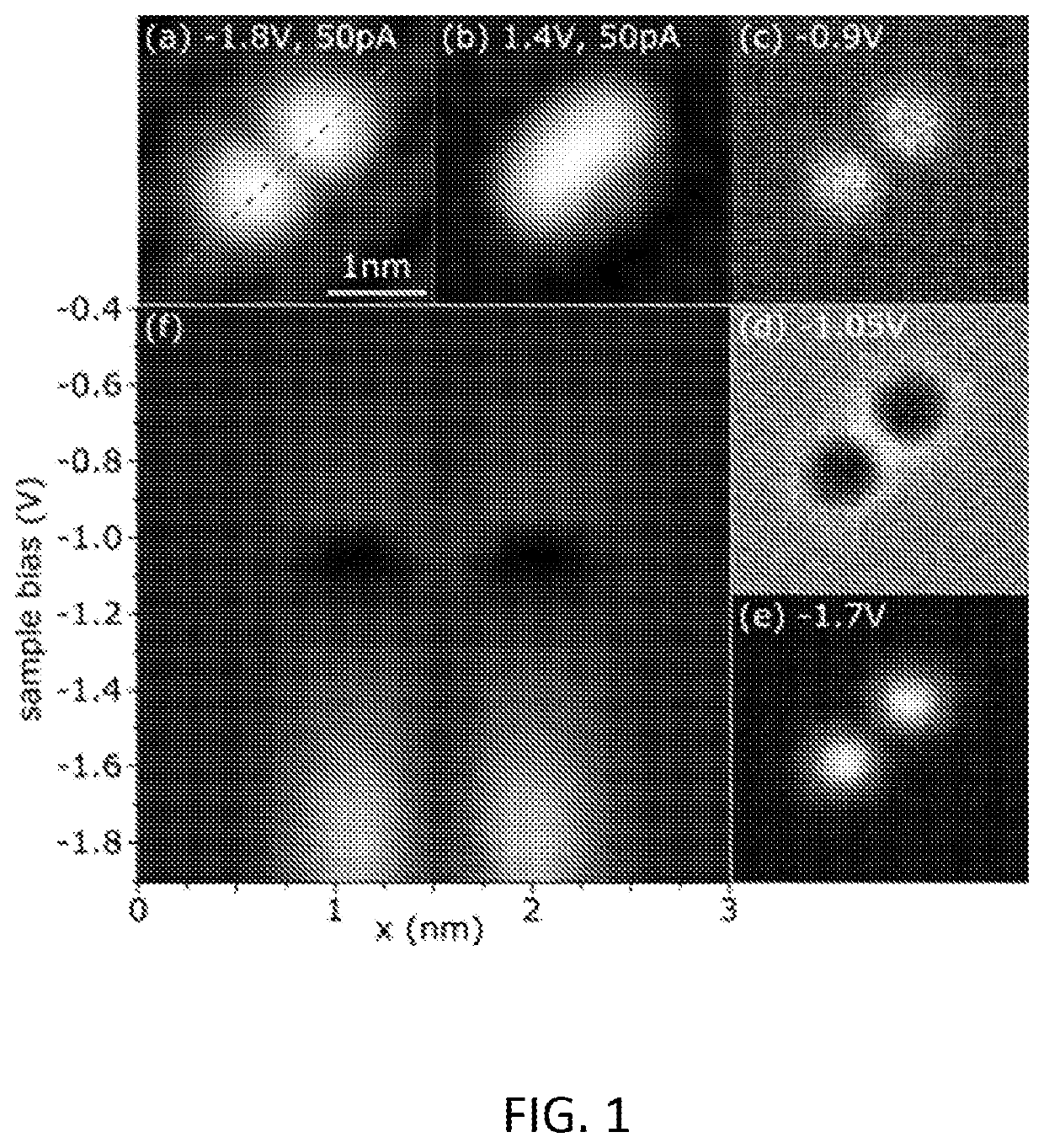
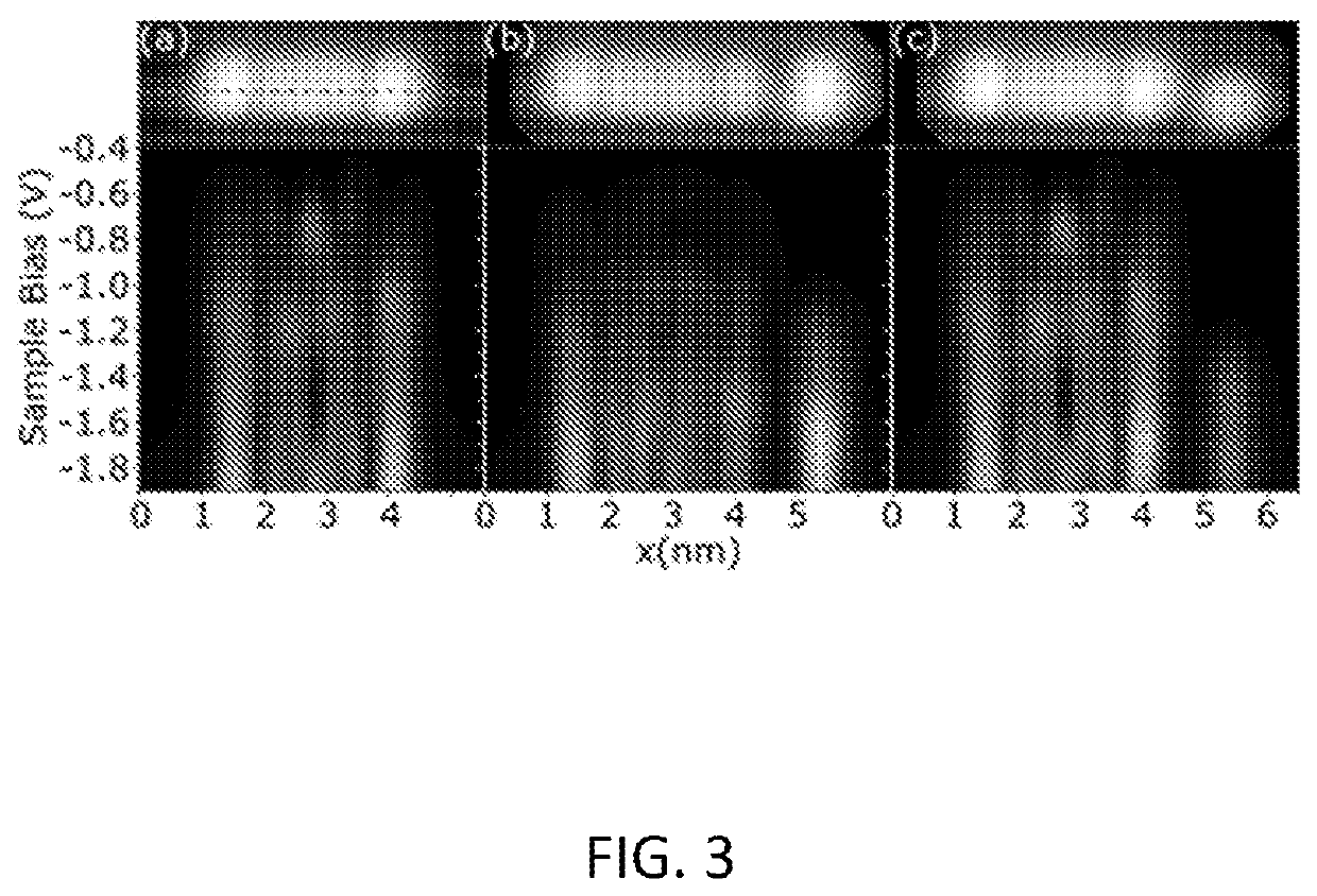
[0081]FIG. 1 shows various characterisations of a linear 3 DB MSiAQD formed along one side of a dimer row on the Si(100) H terminated surface.

[0082]The large dI / dV vs position graphic conveys much information about the energy and spatial distribution of local state density. In other words, it shows where electrons are localized, and not, at each energy probed.

[0083]At most energies, strikingly, little state density is observed at the central atom position. This is a great and clear departure from the single ASiQD result. It clearly shows the emergent molecule like spectroscopy of the ensemble resulting from quantum mechanical overlap of atomic like orbitals.

[0084]Close space DBs form substantial electron sharing bonds. The newly emergent electronic structure is observed in multiple modes of imaging with a scanning tunneling microscope (STM). Spatially point specific dI / dV spectra show pronounced changes indicating new electronic structure. Whole 2D images of dI / dV, taken at a specif...

example 2

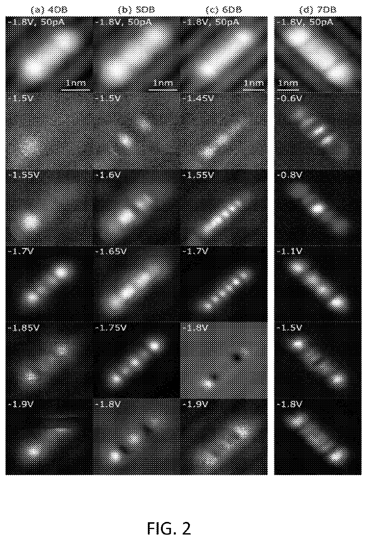
[0103]This experiment shows the ability to form more complex and advanced atom scale electronic structures from multiple ASiQDs according to further embodiments of the present invention. Such structures have utility in binary computation or atomic binary logic.

[0104]FIG. 6A shows a constant current STM image of an ASiQD created by tip-induced desorption of a single hydrogen atom from the H—Si(100) surface. At relatively high voltages (e.g. −1.7 V), the negatively charged ASiQD appears in filled states images as a bright protrusion surrounded by a characteristic small dark halo (17). In the corresponding frequency shift map at 0 V (FIG. 6D)), hydrogen atoms decorating underneath silicon atoms appear as bright protrusions arranged in the 2×1 surface reconstruction. The ASiQD shows up as a dark feature indicating a much higher tip-sample attractive interaction (19).

[0105]FIG. 6C shows I(V) spectroscopy curves taken above the ASiQD and H—Si surface, with both the surface and ASiQD showi...

experiment 3

reating an ASiQD

[0119]Inventive ASiQDs are formed using an inventive process in which vertical manipulation of a single H atom using the tip of an AFM sensor and its application in characterizing and engineering silicon DB-based structures of relevance to nanoelectronic devices. Following a localized tip induced excitation on the Si—H surface, a single hydrogen atom is desorbed and may be either deposited on the surface with stable imaging in STM and AFM, or transferred to the tip apex. The single H atom functionalized tip is identified through a unique signature in frequency shift vs. displacement curves (i.e. Δf(z)) and a characteristic enhancement of STM images in filled and empty states. By bringing the H-functionalized tip apex very close to a DB in the absence of bias and current, a covalent bond between the single hydrogen and silicon atoms is formed. Subsequent changes in the STM images and Δf(z) curves confirm that this mechanically induced reaction results in the passivati...


PUM


Abstract

A multiple-atom silicon quantum dot is provided that includes multiple dangling bonds on an otherwise H-terminated in silicon surface, each dangling bonds having one of three ionization states of +1, 0 or −1 and corresponding respectively to 0, 1, or 2 electrons in a dangling bond state. The dangling bonds together in close proximity and having the dangling bond states energetically in the silicon band gap with selective control of the ionization state of one of the dangling bonds. A new class of electronics elements is provided through the inclusion of at least one input and at least one output to the multiple dangling bonds. Selective modification or creation of a dangling bond is also detailed.

Description

FIELD OF THE INVENTION[0001]The present invention is directed generally to multiple dangling bonds (DBs) on an otherwise H-terminated silicon surface that form quantum dots and in particular to devices based on the modulation of the occupation state of a DB on such a quantum dot.BACKGROUND[0002]Using scanning probe microscopy techniques, inducing and visualizing chemical reactions at the atomic scale is routinely achievable. In the framework of so-called mechanochemistry, (1) mechanical force induced reactions have been studied using NCAFM. (2) Recent works reported force induced atomic-scale switching, (3) quantitative force measurements to induce the diffusion of single atoms (4) and molecules, (5) as well as studying molecular conformers (6) and tautomerization. (7) Other studies have shown examples of mechanically induced vertical manipulation of single atoms. (8, 9) However, direct observation of mechanically induced covalent bonding of two different atoms using NC-AFM remain s...

Claims


Application Information

Patent Timeline
IPC IPC(8): H01L45/00H01L27/24
CPCH01L27/2463B82Y30/00H01L45/10B82Y10/00B82B1/00B82B1/008B82B3/00B82Y20/00C09K11/59C01B33/00H01L29/127H01L29/16H01L29/34H01L29/7613H01L29/66977H01L29/66439Y10S977/937Y10S977/933Y10S977/754H10B63/80H10N70/25H10N99/05
Inventor C, ROBERT A.ACHAI, ROSHANHUFF, TALEANALABIDI, HATEMLIVADARU, LUCIANPIVA, PAULRASHIDI, MOHAMMAD
Owner QUANTUM SILICON INC
Why Eureka
Try Eureka