Method of preventing charge loss from a floating gate
- Summary
- Abstract
- Description
- Claims
- Application Information
AI Technical Summary
Benefits of technology
Problems solved by technology
Method used
Image

Examples
Embodiment Construction
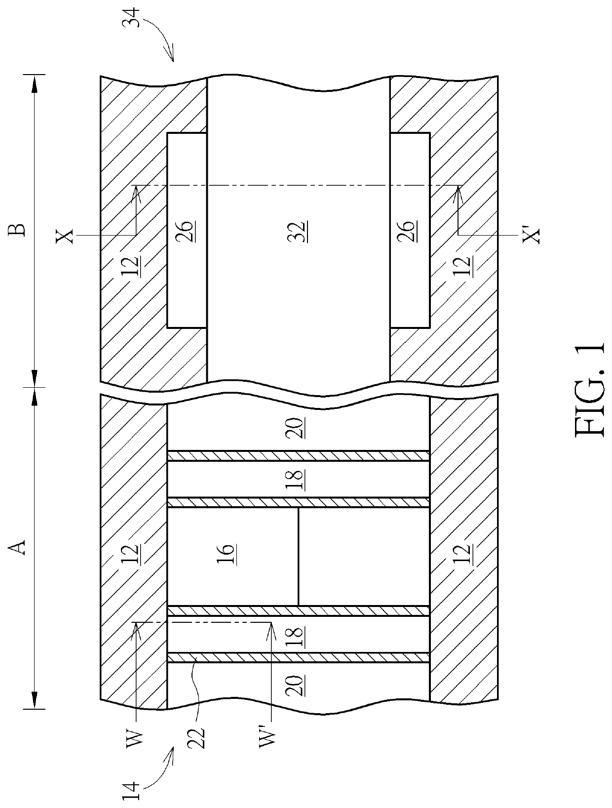
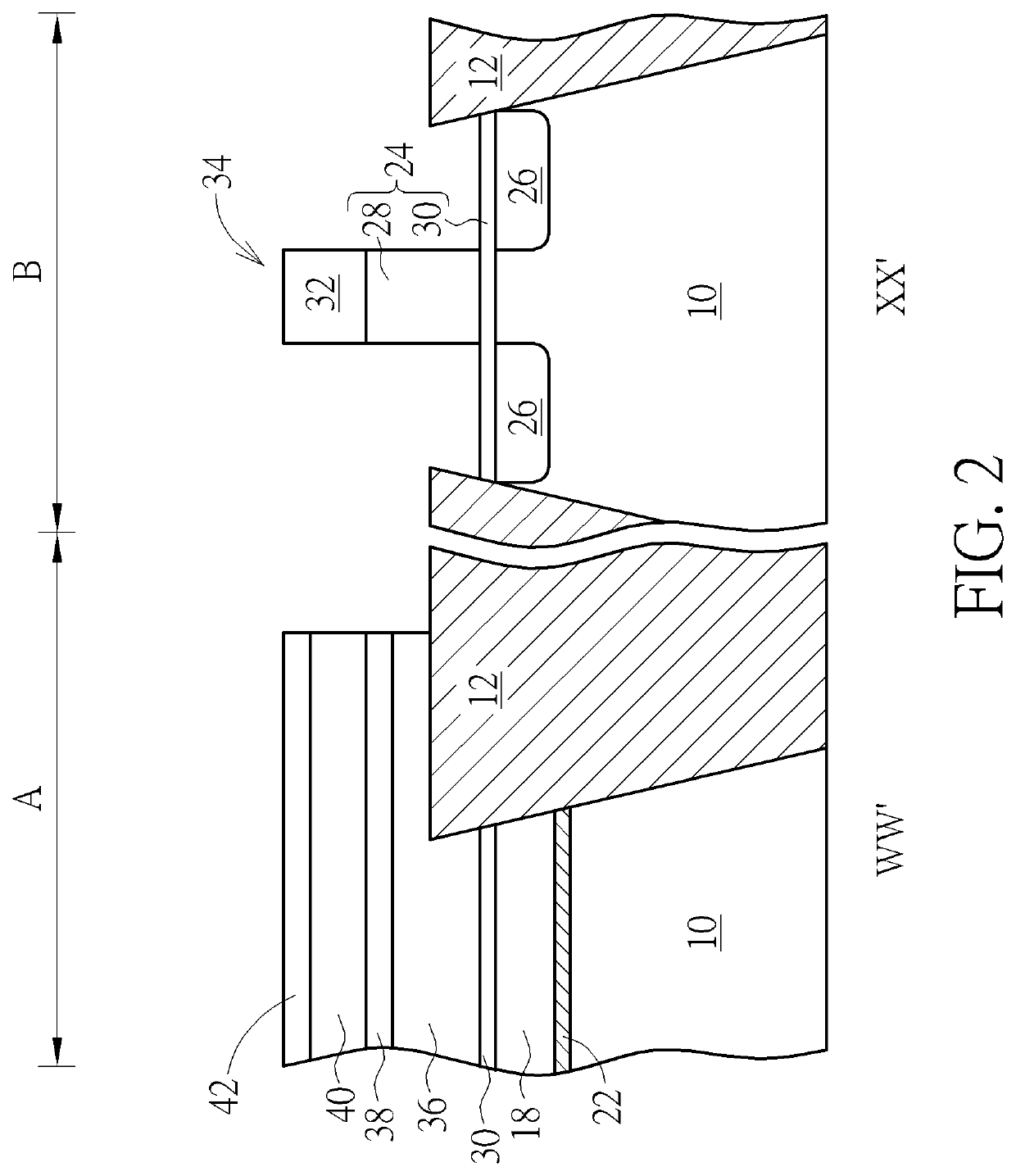
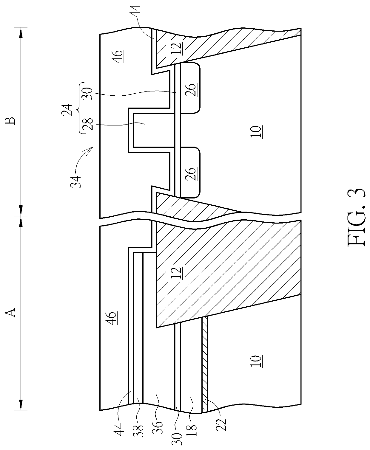
[0020]FIG. 1 to FIG. 10 depict a method of preventing charges loss in a floating gate according to a preferred embodiment of the present invention. FIG. 2 is a sectional view taken along line WW′ and line XX′ in FIG. 1.
[0021]As shown in FIG. 1 and FIG. 2, a substrate 10 is provided. The substrate 10 of the present invention is a bulk silicon substrate, a germanium substrate, a gallium arsenide substrate, a silicon germanium substrate, an indium phosphide substrate, a gallium nitride substrate, a silicon carbide substrate, or a silicon on insulator (SOI) substrate. The substrate 10 is divided into a memory cell region A and a logic region B. A shallow trench isolation (STI) 12 is embedded in the substrate 10 to define active regions in the memory cell region A and the logic region B. The shallow trench isolation 12 may include silicon oxide. A memory cell 14 such as a flash cell is disposed in the memory cell region A. The memory cell 14 includes an erase gate 16, two floating gates ...
PUM
 Abstract
Description
Claims
Application Information
 - R&D Engineer
- R&D Manager
- IP Professional
- Industry Leading Data Capabilities
- Powerful AI technology
- Patent DNA Extraction
Browse by: Latest US Patents, China's latest patents, Technical Efficacy Thesaurus, Application Domain, Technology Topic.
© 2024 PatSnap. All rights reserved.Legal|Privacy policy|Modern Slavery Act Transparency Statement|Sitemap