Method for manufacturing alkali-free glass substrate and alkali-free glass substrate
a technology of alkali-free glass and substrate, which is applied in the field of alkali-free glass substrate, can solve the problems of difficult to obtain flat panel display having desired electric performance, difficult to obtain desired electric performance, and high thermal shrinkage rate, and achieve low thermal shrinkage rate, high strain point, and the effect of a fine circuit pattern
- Summary
- Abstract
- Description
- Claims
- Application Information
AI Technical Summary
Benefits of technology
Problems solved by technology
Method used
Image
Examples
example
Example 1
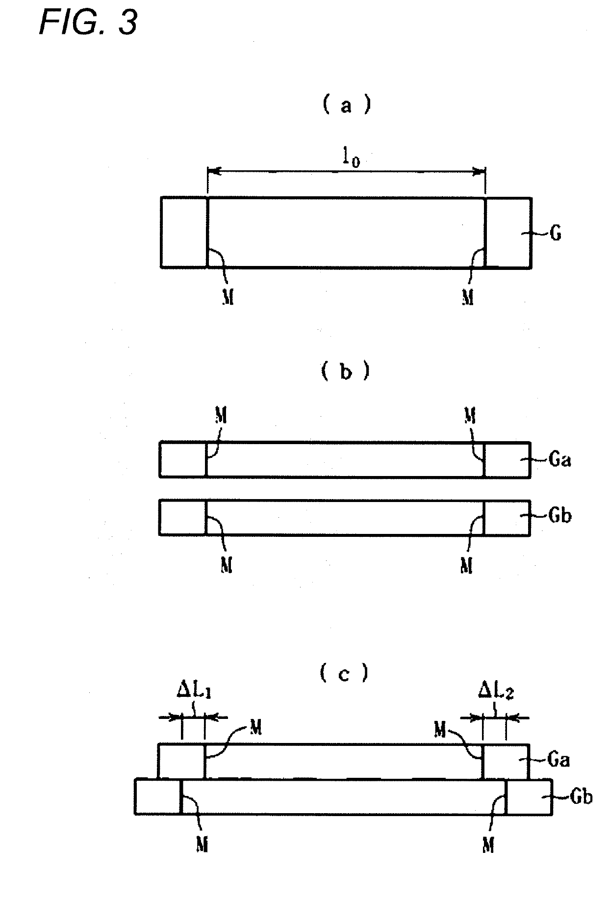
[0116]Examples of the manufacturing method according to the present invention will be described below. FIG. 2 is an explanatory diagram showing a schematic configuration of a preferred glass manufacturing device 1 for performing the manufacturing method according to the present invention.
[0117]First, a configuration of the glass manufacturing device will be described. The glass manufacturing device 10 includes: a melting furnace 1 which electrically melts the raw material batch; a fining tank 2 provided downstream of the melting furnace 1; an adjusting tank 3 provided downstream of the fining tank 2, a forming device 4 provided downstream of the adjusting tank 3. The melting furnace 1, the fining tank 2, the adjusting tank 3, and the forming device 4 are connected by connection flow paths 5, 6, and 7, respectively.
[0118]The melting furnace 1 includes a bottom wall, a side wall, and a ceiling wall, each of which is formed of a high zirconia-based refractory such as ZrO2 elec...
example 2
[0134]Next, the glass manufactured by using the method according to the present invention will be described. Tables 1 to 6 show Examples (No. 1 to 4, 8 to 27, 29 to 39) and Comparative Examples (No. 5 to 7, 28, 40 to 42) of the present invention.
TABLE 1No.1234567Glass CompositionSiO261.161.161.161.161.161.161.1(Mass %)Al2O318.618.618.618.618.618.618.6B2O30.70.70.70.70.70.70.7MgO3.23.23.23.23.23.23.2CaO5.15.15.15.15.15.15.1SrO0.60.60.60.60.60.60.6BaO10.410.410.410.410.410.410.4P2O50000000ZrO20.0200.0200.0400.0300.1000.0200.020TiO20.1000.0030.0030.0040.0040.0030.100SnO20.1900.2200.2100.2200.2200.2100.190Fe2O30.0100.0140.0130.0140.0130.0140.010Cr2O30.00010.00010.00010.00010.00010.00010.0001SO30.00030.00030.00030.00030.00040.00030.0003β-OH ( / mm)0.060.050.050.070.120.090.06Strain Point (° C.)750750750749747748750Thermal Shrinkage Rate (ppm)10101010111010Bubble enlarging Temperature (° C.)1610160516101590164516351635Maximum Temperature of Fining1630163016251630163016251620Tank (° C.)Maxim...
PUM
| Property | Measurement | Unit |
|---|---|---|
| Temperature | aaaaa | aaaaa |
| Temperature | aaaaa | aaaaa |
| Temperature | aaaaa | aaaaa |
Abstract
Description
Claims
Application Information

