Image sensor and image capture device
a technology of image sensor and image, which is applied in the direction of color television, television system, radio control device, etc., can solve the problem of not being able to process the signals outputted from all of the photodiodes simultaneously at high speed
- Summary
- Abstract
- Description
- Claims
- Application Information
AI Technical Summary
Benefits of technology
Problems solved by technology
Method used
Image

Examples
first embodiment
The First Embodiment
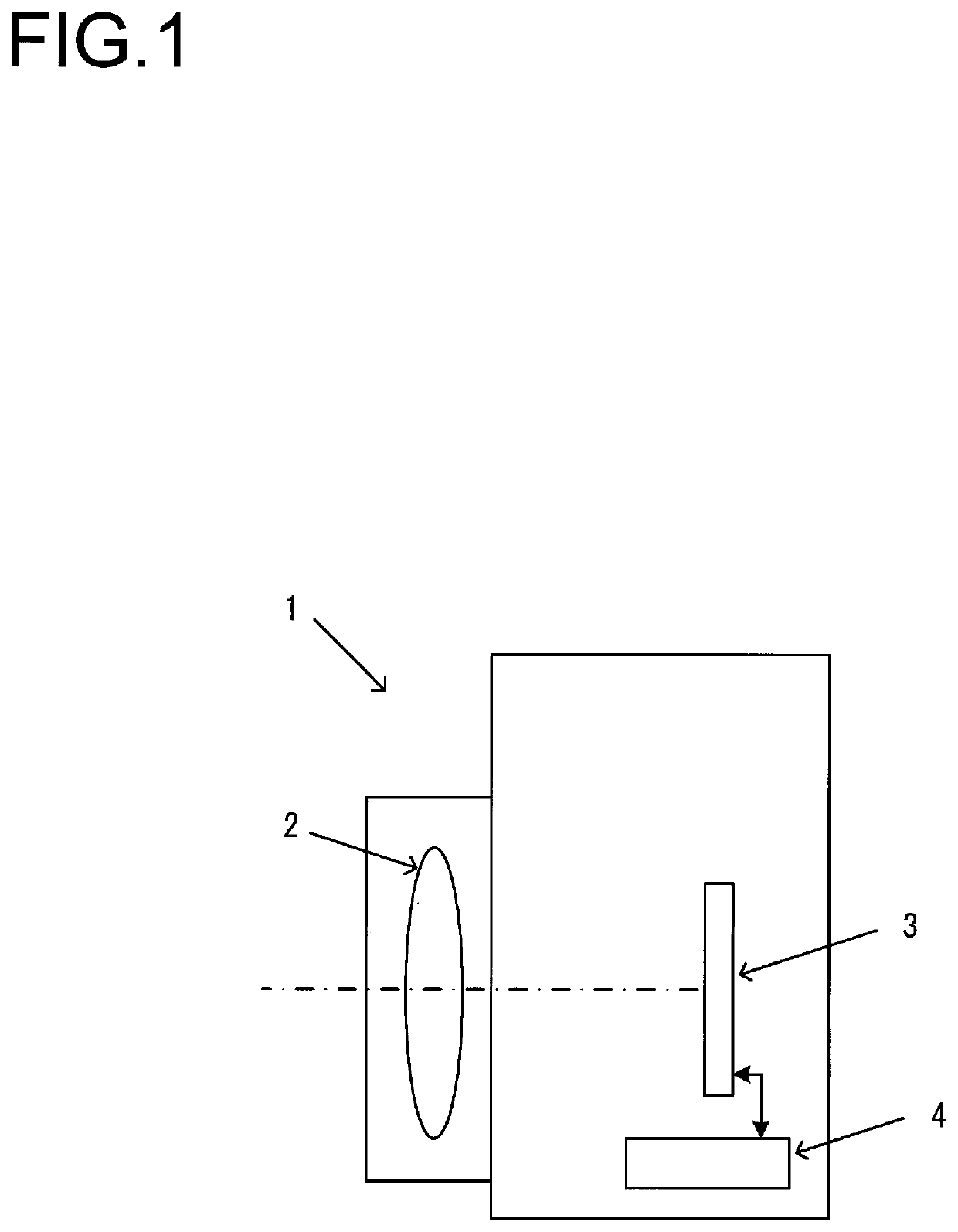
[0020]FIG. 1 is a block diagram showing the structure of an image capture device according to a first embodiment. The image capture device 1 comprises a photographic optical system 2, an image sensor 3, and a control unit 4. This image capture device 1 may, for example, be a camera. The photographic optical system 2 focuses an image of a photographic subject upon the image sensor 3. The image sensor 3 generates an image signal by capturing the image of the photographic subject that has been focused by the photographic optical system 2. The image sensor 3 may, for example, be a CMOS image sensor. The control unit 4 outputs a control signal to the image sensor 3 for controlling the operation of the image sensor 3. Moreover, the control unit 4 functions as an image generation unit that generates image data by performing image processing of various kinds upon the image signal outputted from the image sensor 3. It should be understood that it would also be acceptable ...
second embodiment
The Second Embodiment
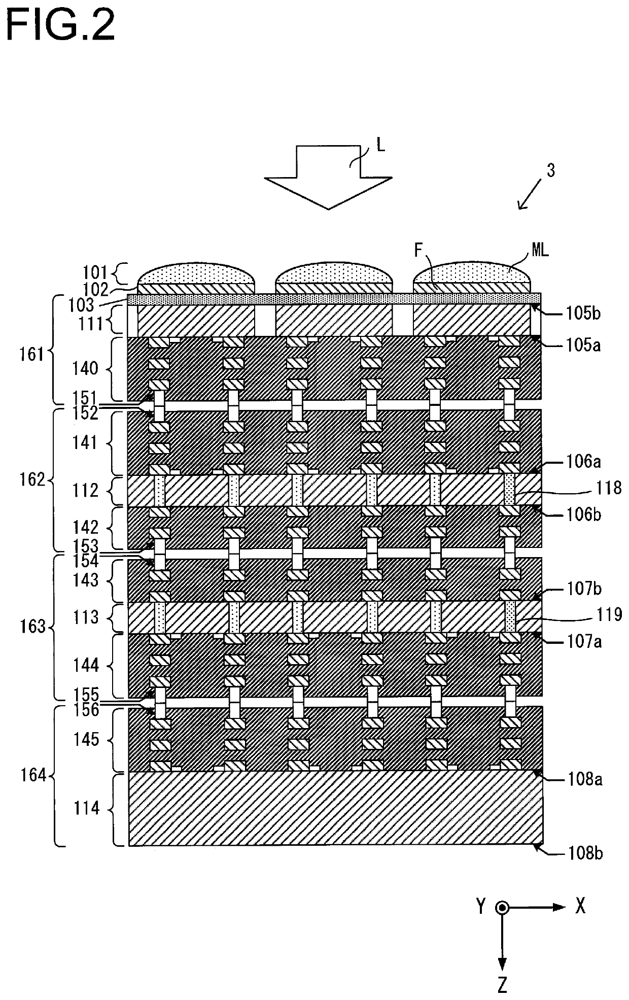
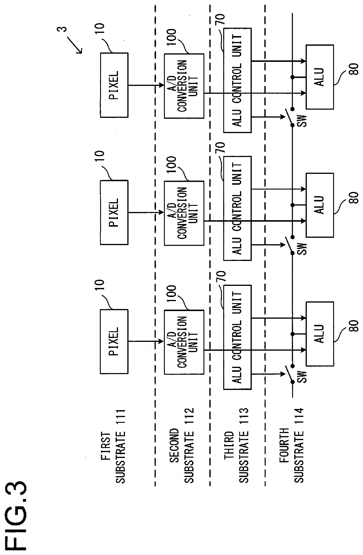
[0063]An image sensor according to a second embodiment of the present invention will now be explained with reference to FIG. 8 and FIG. 9. It should be understood that, in the figures, portions that are equivalent to portions of the first embodiment are denoted by the same reference symbols, and that this explanation will principally concentrate upon the features of difference from the image sensor of the first embodiment. FIG. 8 is a block diagram showing the structure of this capture element according to the second embodiment. A first substrate 111 includes a plurality of pixels 10 arranged in a two dimensional array, and a second substrate 112 includes a plurality of comparison units 30. The comparison units 30 compare the signals outputted from the pixels with reference signals, and output the results of these comparisons to a third substrate 113 and to a fourth substrate 114.
[0064]The third substrate 113 includes a plurality of first storage units 50. And t...
third embodiment
The Third Embodiment
[0075]An image sensor according to a third embodiment of the present invention will now be explained with reference to FIG. 10 and FIG. 11. It should be understood that, in the figures, portions that are equivalent to portions of the first and second embodiments are denoted by the same reference symbols, and that this explanation will principally concentrate upon the features of difference from the image sensors of the first and second embodiments. FIG. 10 is a block diagram showing the structure of an A / D conversion unit 100 included in this capture element according to the third embodiment. This A / D conversion unit 100 comprises a comparison unit 300, a first storage unit 50, a second storage unit 60, and a level conversion unit 180 (i.e. a level shifter).
[0076]The level conversion unit 180 comprises a first capacitor C1, a second capacitor C2, and a buffer 130 (i.e. an amplification unit). The level conversion unit 180 converts the voltage level of the output ...
PUM
 Abstract
Description
Claims
Application Information
 - R&D
- Intellectual Property
- Life Sciences
- Materials
- Tech Scout
- Unparalleled Data Quality
- Higher Quality Content
- 60% Fewer Hallucinations
Browse by: Latest US Patents, China's latest patents, Technical Efficacy Thesaurus, Application Domain, Technology Topic, Popular Technical Reports.
© 2025 PatSnap. All rights reserved.Legal|Privacy policy|Modern Slavery Act Transparency Statement|Sitemap|About US| Contact US: help@patsnap.com