Highly stable organic light-emitting panel

a technology of organic light-emitting panels and oled plates, which is applied in the field of oled plates, can solve the problems of damage to the quality and reliability of oled devices, the organic layer between anodes and cathodes may become thinner than in other portions, so as to reduce the burn area of surrounding pixel, improve the reliability of the panel, and prevent the effect of heat generation

Active Publication Date: 2020-09-10
GUAN YEOLIGHT TECH CO LTD
View PDF0 Cites 2 Cited by
  • Summary
  • Abstract
  • Description
  • Claims
  • Application Information

AI Technical Summary

Benefits of technology

[0036]A. In the present invention, the substrate is provided with an auxiliary electrode, each of the plurality of pixelated OLED circuit assemblies is connected to a circuit protection structure, and all of the circuit protection structures are electrically connected to the auxiliary electrode on the substrate. Each circuit protection structure is independently provided with a fusing condition, and quick fusing can be realized by selecting suitable short circuit current affected by a pixel with short-circuit defect. When one or more of the OLED circuit assemblies on the substrate encounter short circuit defect, its corresponding circuit protection structure will fuse in time, thereby isolating the OLED circuit assembly having the short circuit defect from normal working OLED circuit assemblies, and preventing the heat generated by fusing of the circuit protection structure from affecting the normal panel pixels, so as to provide real time protection to the panel and improve the reliability of the panel.
[0037]B. In the present invention, a joule heat fusible fuse is adopted, and an influence area of the thermal energy of the pixel with short-circuit defect is defined. By amplifying the ratio of the short-circuit point current to the normal pixel current, the short-circuit prevention design can realize real-time fuse and minimize the burn area of the surrounding pixel. At the same time, the panel is provided with at least 100 pixelated OLED circuit assemblies, so as to ensure that current of the short-circuit point is at least 100 times different from the normal pixel current, and that the circuit protection structure will protect the whole OLED circuit assemblies when sudden fluctuations occur.
[0038]C. In the present invention, each circuit protection structure is respectively connected in series with a second resistance protector between the pixelated first electrode in each of the pixelated OLED circuit assemblies and the auxiliary electrode. The circuit protection structure is adapted to provide protection to the panel when short-circuit defect occurs in a pixel due to low resistance fault in the pixelated OLED circuit assemblies, and the second resistance protector is adapted to provide protection to the panel when short-circuit defect occurs in a pixel due to medium / high resistance fault in the pixelated OLED circuit assemblies, such that the present invention can provide short circuit prevention protect when different types of short circuit defects occur in the OLED circuit assemblies, thereby improving the reliability of the panel.
[0039]D. In a preferred embodiment of the present invention, the auxiliary electrode, low resistance fault protector, high resistance fault protector and the first electrode are sequentially connected in series. The combination of the low resistance fault protector and high resistance fault protector can effectively protect the panel under different conditions, thereby ensuring the reliability of the panel. At the same time, the influence of different types of defects on the panel is fully considered, and different parameters for different short circuit prevention design in units are proposed. An insulating material is covered on the auxiliary electrode—low resistance fault protector —high resistance fault protector, thereby preventing forming short circuit with the second electrode which will cause panel failure. The low resistance fault protector can simultaneously provide protection when the defect point occurs in the high resistance fault protector area or the luminous area, thereby helping to increase the yield. At the same time, the high resistance fault protector can provide effective protection when a short circuit occurs in a pixel region due to high resistance fault, and shall not fuse when the generated short circuit current gain is less than 300 or the current is less than 5 mA. Therefore, the high resistance fault protector in pixel with big resistance defect is designed to be in parallel connection with other normal pixel, and the panel can work normally as long as the total current of the normal pixels account for 97% or more of the total current.
[0040]E. Since the second resistance protector accounts for 5% to 30% of the pixel area of the pixelated OLED circuit assemblies, depending on the resistance of the designed second resistance protector and the process capability, there is a probability that the second resistance protector may also encounter short-circuit defects. When short circuit defects occur in the region of the second resistance protector and results in failure of the second resistance protector, the circuit protection structure can provide effective protection to more than 99% pixel area of the pixelated OLED circuit assemblies (including light emitting area and the second resistance protector). Therefore, the series connected circuit protection structure and the second resistance protector can not only provide protection when short-circuit point of high and low resistance defects occur, but also provide protection when the second resistance protector and pixelated OLED circuit assemblies encounter short circuit defects, thereby effectively solving the problem that prior art technology cannot provide protection “when the resistance protector encounters defects.”

Problems solved by technology

There are inevitably dust particles, burrs, pinholes, cracks and other defects in the manufacture process of OLED panels.
As a result, the anode and cathode may come into direct contact and cause defects (called short-circuit points), or the organic layer between the anode and cathode may become thinner than in other portions.
When an OLED device is in operation, the current tends to pass through the short-circuit points rather than other portions, causing heat accumulation at the short-circuit points, thus causing damage to the quality and reliability of the OLED device.
Under same conditions, the larger the illumination area of the OLED panel, the greater the possibility of occurrence of short-circuit point.
It is possible to reduce the short-circuit points by increasing the thickness of the organic layer, but this requires higher driving voltage of the OLED device, thus affecting the device efficiency.
Moreover, it cannot completely eliminate the short-circuit points.
If the above two necessary conditions cannot be met, the short-circuit prevention effect will not be obvious, and the short circuit point will generate high heat due to high current (P=I2R; P=power, I=current, R=resistance), thereby reducing its reliability.
However, most of the power supply devices cannot meet this requirement.
Furthermore, most of the OLED devices have a power supply of constant current, and the above short circuit protection mechanism will result in a large amount of failure current (i.e. the current passing through the short circuit points (current of normal OLED device under effective supply+failure current at short circuit points=total output current of a constant current power supply)) at the short circuit points, thereby reducing the photoelectric performance of the panel.
If the resistance of the circuit protection structure is large enough to match with the equivalent resistance of a pixel, the circuit protection design can be achieved in the form of series resistance, However, as calculated the equivalent resistance of a pixel is usually tens to hundreds of thousands of ohm, which is usually far higher than the resistance of the circuit protection structure, so there will be a high percentage of current passing through the short circuit points, causing significant change in light efficiency of the entire panel.

Method used


Image

  • Highly stable organic light-emitting panel
  • Highly stable organic light-emitting panel
  • Highly stable organic light-emitting panel

Examples


example 1

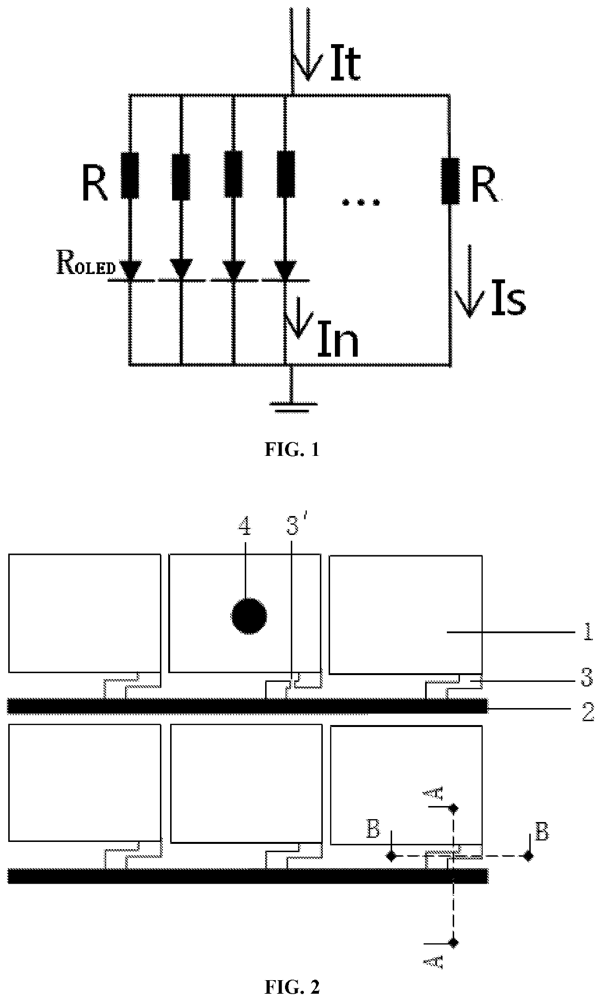
[0066]OLED panels are provided, each having a pixel number of 10000, an operation voltage of 6V and a corresponding current of 100 mA. Fuses having resistance of 30 Ω, 60Ω, 200Ω, 600Ω are respectively connected in series with each of the pixelated OLED circuit assemblies, and each pixel has an average current J of 0.01 mA. When a complete short circuit defect point appears, the current Is of the pixel with short-circuit defect is 66.6 mA, 50.0 mA, 23.1 mA and 9.1 mA according to different resistance design, and the corresponding coefficient Is / J is 6667, 5000, 2308 and 909 respectively. The smaller the value of Is / J is, the more difficult to reach the fusing condition of the fuse. Experiments indicate that the fuse will not reach fusing condition until the entire panel is burn when the fuse has a resistance of 600Ω. At the same time, the influenced area of surrounding pixels due to the joule heat of the fuse has a diameter of about 50 μm, 100μm, >500 μm and panel failure respectivel...

example 2

[0067]An OLED panel is provided, having a pixel number of 100, an operation voltage of 6V and a corresponding current of 100 mA. Fuses of 30 Ω, 60Ω, 200Ω, 600Ω are respectively connected in series with each of the pixelated OLED circuit assemblies, and each pixel has an average current J of 1 mA. When a short circuit defect point appears, the current Is of the pixel with short-circuit defect is 67.0 mA, 50.4 mA, 23.3 mA and 9.22 mA according to different resistance design, and the corresponding coefficient Is / J is 67.0, 50.4, 23.3 and 9.22 respectively. The smaller the value of Is / J is, the more difficult to reach the fusing condition of the fuse. Experiments indicate that the fuse will not reach fusing condition until the entire panel is burn when the fuse has a resistance of 600Ω At the same time, the influenced area of surrounding pixels due to the joule heat of the fuse has a diameter of about 50 μm, 100 μm, >500 μm and panel failure respectively. Therefore, increasing the coeff...

example 3

Short Circuit Protection for Small Sized Panel (Small Current of 10 to 30 mA)

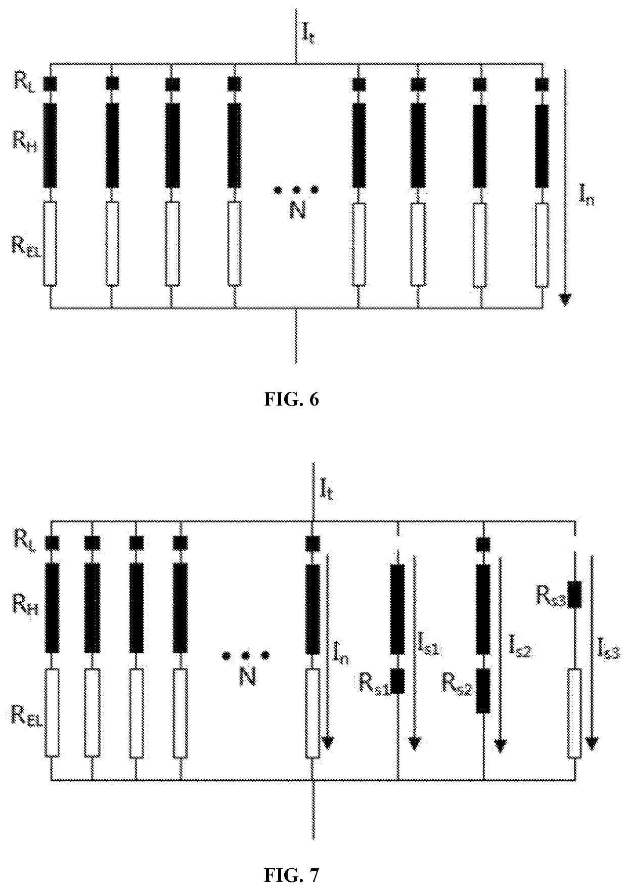
[0093]OLED panels herein used have a voltage of 6V and a current density for each pixel of 0.0126 mA. The number of pixels is 800, 1600, 2400, respectively, and the corresponding area is 144 mm2 to 433 mm2. The low resistance fault protector is a metal conductive material with a melting point of 800° C., and has a conductor width of 0.1 un or a conductor thickness of 10 nm. An insulation layer having a melting point of 400° C. is arranged on the substrate below the low resistance fault protector. The resistance of the low resistance fault protector in multiple units can be ignored. The high resistance fault protector has a sheet resistance of 50Ω / □, with different aspect ratios, and the corresponding equivalent resistance is 500Ω, 1000Ω, 5000Ω, 10000Ω. The short-circuit points are supposed to have an equivalent impedance of A-0Ω, B-100Ω, C-500Ω, D-1000Ω and E-5000Ω, respectively. The experimental results ar...


PUM

PropertyMeasurementUnit
diameteraaaaaaaaaa
thicknessaaaaaaaaaa
widthaaaaaaaaaa

Abstract

A highly stable organic light-emitting panel includes a substrate and a plurality of pixelated OLED circuit assemblies. The substrate further includes an auxiliary electrode and a plurality of circuit protection structures, each of which is electrically connected to a corresponding pixelated first electrode in each pixelated OLED circuit assembly. The plurality of circuit protection structures are respectively connected to the auxiliary electrode. An insulator covers the auxiliary electrode, the plurality of circuit protection structures, and an area between the plurality of circuit protection structures and the plurality of OLED circuit assemblies. When a current passing through a pixel with short-circuit defect in any one of the plurality of OLED circuit assemblies is greater than a predetermined threshold of the circuit protection structure, the circuit protection structure corresponding to the pixel with short-circuit defect fuses, thereby isolating the OLED circuit assembly corresponding to the pixel with short-circuit defect.

Description

TECHNICAL FIELD[0001]The present invention relates to the technical field of OLED panel, in particular to a highly stable OLED panel.BACKGROUND OF THE INVENTION[0002]There are inevitably dust particles, burrs, pinholes, cracks and other defects in the manufacture process of OLED panels. The distance between the anode and cathode of an OLED panel is usually very small (about tens to hundreds of nanometers). As a result, the anode and cathode may come into direct contact and cause defects (called short-circuit points), or the organic layer between the anode and cathode may become thinner than in other portions. When an OLED device is in operation, the current tends to pass through the short-circuit points rather than other portions, causing heat accumulation at the short-circuit points, thus causing damage to the quality and reliability of the OLED device.[0003]Under same conditions, the larger the illumination area of the OLED panel, the greater the possibility of occurrence of short...

Claims


Application Information

Patent Timeline
Patent Type & Authority Applications(United States)
IPC IPC(8): H01L27/32F21V25/04F21V23/06
CPCF21V23/06F21Y2115/15F21V25/04H01L27/329F21S8/00F21V23/003H10K59/131H10K2102/341H10K59/1795
Inventor LEE, YUZHU, YINGGUANGXIE, JINGYU, QIANQIANGUO, LIXUEHU, YONGLAN
Owner GUAN YEOLIGHT TECH CO LTD
Why Eureka
Try Eureka